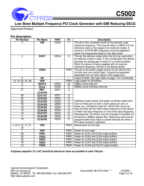
Description
Pin Number 2 Pin Name XIN PWR VDDA I/O I Description This pin is the connection point for the devices Loop reference frequency.
This may be either a CMOS 3.3 volt reference clock or the output of an external crystal.
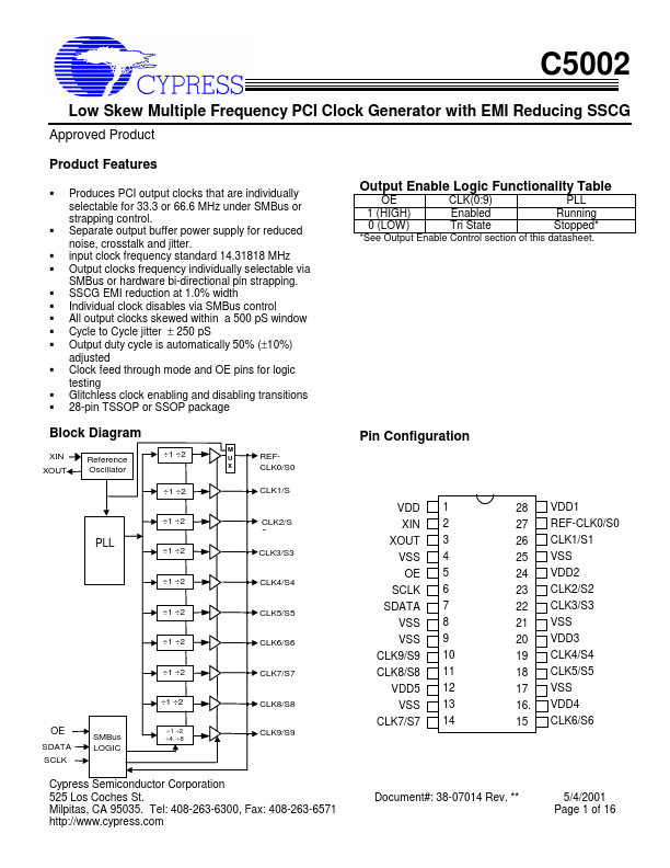
Features
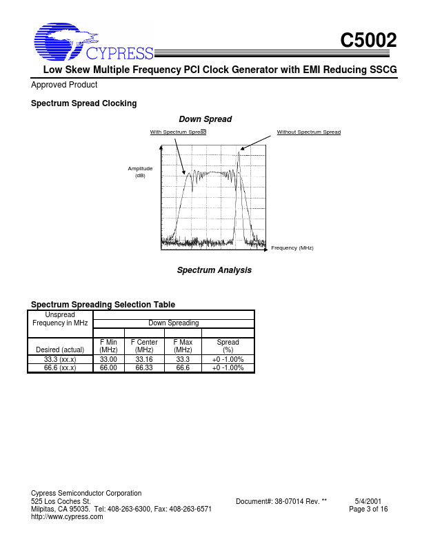
- Produces PCI output clocks that are individually selectable for 33.3 or 66.6 MHz under SMBus or strapping control. Separate output buffer power supply for reduced noise, crosstalk and jitter. input clock frequency standard 14.31818 MHz Output clocks frequency individually selectable via SMBus or hardware bi-directional pin strapping. SSCG EMI reduction at 1.0% width Individual clock disables via SMBus control All output cloc.
 C5002 Datasheet