ICS9LPRS535
Description
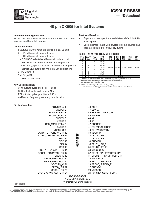
4 5 6 7 8 9 10 PCI_F5/ITP_EN GNDPCI VDD48 USB_48MHz/FSLA GND48 VDD96_IO DOT96T_LPR/SRCT0_LPR 3.3V PCI clock output or CR#_A input. To configure this pin as CR#_A, the PCI output must first be disabled in Byte 2, bit 0.
Key Features
- Integrated Series Resistors on differential outputs
- 2 - CPU differential push-pull pairs
- 4 - SRC differential push-pull pairs
- 1 - CPU/SRC selectable differential push-pull pair
- 1 - SRC/DOT selectable differential push-pull pair
- 1- SRC/Stop_Inputs selectable differential push-pull pair
- 1 - 25MHz SE1 output for Wake-on-Lan applications
- 3 - PCI, 33MHz
- 1 - USB, 48MHz
- 1 - REF, 14.31818MHz Key Specifications