Datasheet Details
| Part number | ICS831742I |
|---|---|
| Manufacturer | Integrated Device Technology |
| File Size | 423.20 KB |
| Description | 4:2 Differential Clock/Data Multiplexer |
| Datasheet |
 ICS831742I Datasheet ICS831742I Datasheet
|
|
|
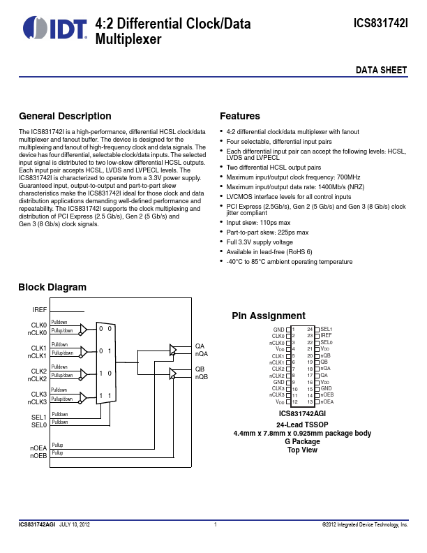
The ICS831742I is a high-performance, differential HCSL clock/data multiplexer and fanout buffer.
The device is designed for the multiplexing and fanout of high-frequency clock and data signals.
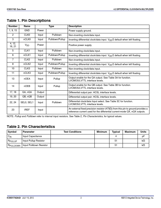
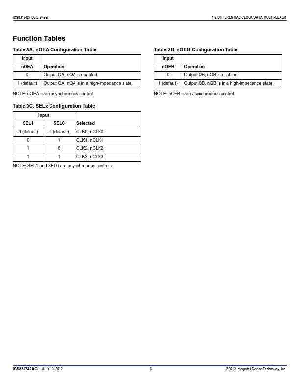
The device has four differential, selectable clock/data inputs.
| Part number | ICS831742I |
|---|---|
| Manufacturer | Integrated Device Technology |
| File Size | 423.20 KB |
| Description | 4:2 Differential Clock/Data Multiplexer |
| Datasheet |
ICS831742I Datasheet
|
|
|
|