SPI42N03S2L-13
SPI42N03S2L-13 is OptiMOS Power-Transistor manufactured by Infineon.
Features
- N-channel
- Enhancement mode
- Logic level
..
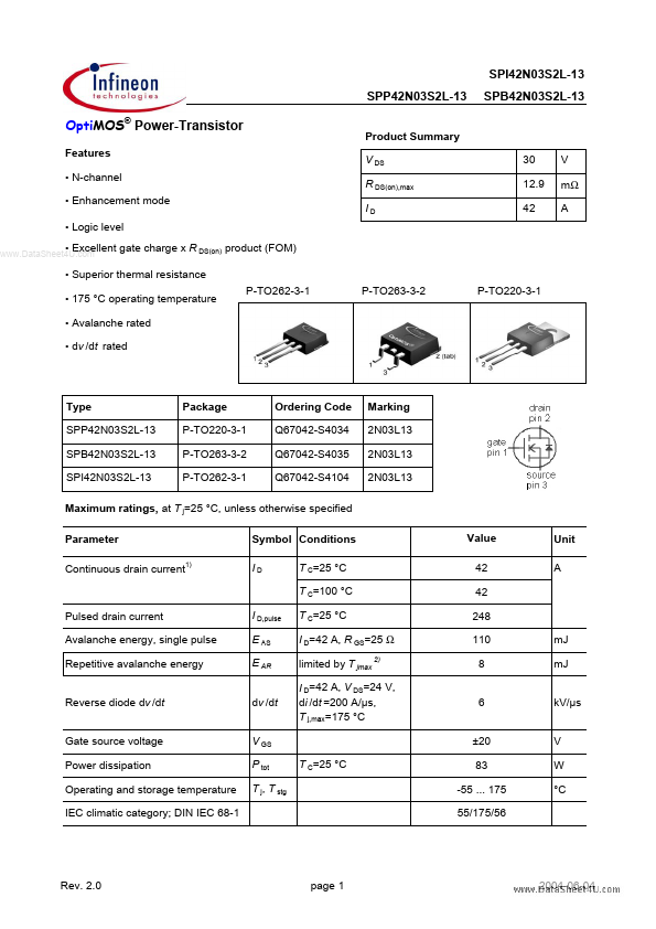
Product Summary V DS R DS(on),max ID 30 12.9 42 V mΩ A
- Excellent gate charge x R DS(on) product (FOM)
- Superior thermal resistance
- 175 °C operating temperature
- Avalanche rated
- dv /dt rated P-TO262-3-1 P-TO263-3-2 P-TO220-3-1
Type SPP42N03S2L-13 SPB42N03S2L-13 SPI42N03S2L-13
Package P-TO220-3-1 P-TO263-3-2 P-TO262-3-1
Ordering Code Q67042-S4034 Q67042-S4035 Q67042-S4104
Marking 2N03L13 2N03L13 2N03L13
Maximum ratings, at T j=25 °C, unless otherwise specified Parameter Continuous drain current1) Symbol Conditions ID T C=25 °C T C=100 °C Pulsed drain current Avalanche energy, single pulse Repetitive avalanche energy Reverse diode dv /dt Gate source voltage Power dissipation Operating and storage temperature IEC climatic category; DIN IEC 68-1 I D,pulse E AS E AR dv /dt V GS P tot T j, T stg T C=25 °C T C=25 °C I D=42 A, R GS=25 Ω limited by T jmax 2) I D=42 A, V DS=24 V, di /dt =200 A/µs, T j,max=175 °C Value 42 42 248 110 8 6 ±20 83 -55 ... 175 55/175/56 m J m J k V/µs V W °C Unit A
Rev. 2.0 page 1
2004-06-04
SPI42N03S2L-13 SPP42N03S2L-13
Parameter Symbol Conditions min. Thermal characteristics Thermal resistance, junction
- case SMD version, device on PCB
..
SPB42N03S2L-13
Unit max.
Values typ.
R th JC R th JA minimal footprint 6 cm2 cooling area3)
- 1.2
- 1.8 62 40
K/W
Electrical characteristics, at T j=25 °C, unless otherwise specified Static characteristics Drain-source breakdown voltage Gate threshold voltage Zero gate voltage drain current V (BR)DSS V GS=0 V, I D=1 m A V GS(th) I DSS V DS=V GS, I D=37 µA V DS=30 V, V GS=0 V, T j=25 °C V DS=30 V, V GS=0 V, T j=125 °C Gate-source leakage current Drain-source on-state resistance4) I GSS R DS(on) V GS=20 V, V DS=0 V V GS=4.5 V, I D=21 A V GS=4.5 V, I D=21 A, SMD version V GS=10 V, I D=21 A V GS=10 V, I D=21 A, SMD version Gate resistance Transconductance RG g fs |V DS|>2|I D|R DS(on)max, I D=42 A 30 1.2 1.6 0.01 2 1 µA V
10 1 14.9...