IPD26CNE8NG
IPD26CNE8NG is Power-Transistor manufactured by Infineon.
- Part of the IPB-26CNE comparator family.
- Part of the IPB-26CNE comparator family.
Features
- N-channel, normal level
- Excellent gate charge x R DS(on) product (FOM)
- Very low on-resistance R DS(on)
- 175 °C operating temperature
- Pb-free lead plating; Ro HS pliant
- Qualified according to JEDEC1) for target application
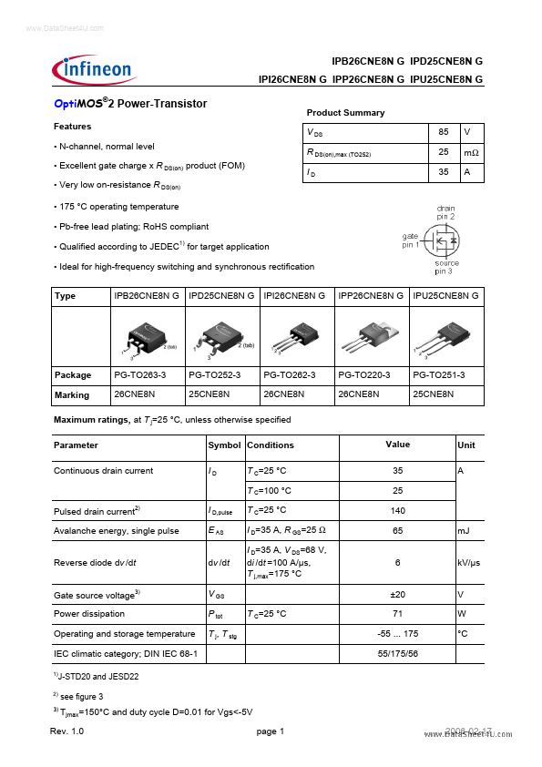
Product Summary V DS R DS(on),max (TO252) ID 85 25 35 V mΩ A
- Ideal for high-frequency switching and synchronous rectification Type IPB26CNE8N G IPD25CNE8N G IPI26CNE8N G IPP26CNE8N G IPU25CNE8N G
Package Marking
PG-TO263-3 26CNE8N
PG-TO252-3 25CNE8N
PG-TO262-3 26CNE8N
PG-TO220-3 26CNE8N
PG-TO251-3 25CNE8N
Maximum ratings, at T j=25 °C, unless otherwise specified Parameter Continuous drain current Symbol Conditions ID T C=25 °C T C=100 °C Pulsed drain current2) Avalanche energy, single pulse Reverse diode dv /dt Gate source voltage3) Power dissipation Operating and storage temperature IEC climatic category; DIN IEC 68-1
1)
Value 35 25 140 65 6 ±20
Unit A
I D,pulse E AS dv /dt V GS P tot T j, T stg
T C=25 °C I D=35 A, R GS=25 Ω I D=35 A, V DS=68 V, di /dt =100 A/µs, T j,max=175 °C m J k V/µs V W °C
T C=25 °C
71 -55 ... 175 55/175/56
J-STD20 and JESD22 see figure 3
2)
3)
Tjmax=150°C and duty cycle D=0.01 for Vgs<-5V page 1 2006-02-17
Rev. 1.0
..
IPB26CNE8N G IPD25CNE8N G IPI26CNE8N G IPP26CNE8N G IPU25CNE8N G
Parameter Symbol Conditions min. Thermal characteristics Thermal resistance, junction
- case Thermal resistance, junction ambient (TO220, TO262, TO263) Thermal resistance, junction ambient (TO252, TO251) R th JC R th JA minimal footprint 6 cm2 cooling area4) minimal footprint 6 cm2 cooling area4) 2.1 62 40 75 50 K/W Values typ. max. Unit
Electrical characteristics, at T j=25 °C, unless otherwise specified Static characteristics Drain-source breakdown voltage Gate threshold voltage Zero gate voltage drain current V (BR)DSS V GS=0 V, I D=1 m A V GS(th) I DSS V DS=V GS, I D=39 µA V DS=68 V, V GS=0 V, T j=25 °C V DS=68 V, V GS=0 V, T j=125 °C Gate-source leakage current Drain-source on-state resistance I GSS R...