Datasheet4U Logo Datasheet4U.com

S26KL512S - 512Mb (64MB) HYPER FLASH

Description

1.1 DDR center aligned read strobe (DCARS) functionality 7 1.2 Error detection and correction functionality 7 2 Connection diagram10 2.1 FBGA 24-ball 5 × 5 array footprint 10 3 Signal description 11 4 HYPERBUS™ protocol

Features

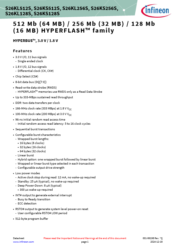
  • 3.0 V I/O, 11 bus signals - Single ended clock.
  • 1.8 V I/O, 12 bus signals - Differential clock (CK, CK#).
  • Chip Select (CS#).
  • 8-bit data bus (DQ[7:0]).
  • Read-write data strobe (RWDS) -.

📥 Download Datasheet

Other Datasheets by Infineon

Full PDF Text Transcription

Click to expand full text
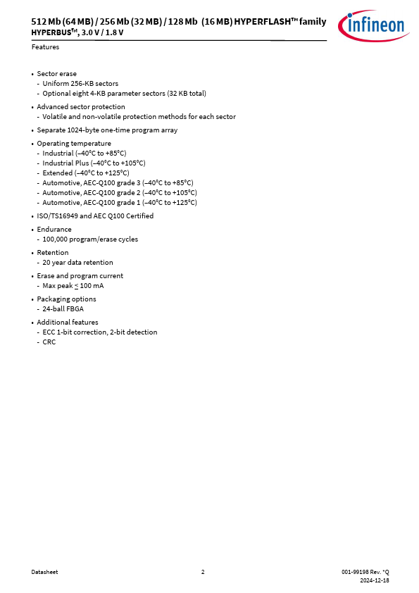
S26KL512S, S26KS512S, S26KL256S, S26KS256S, S26KL128S, S26KS128S 512 Mb (64 MB) / 256 Mb (32 MB) / 128 Mb (16 MB) HYPERFLASH™ family HYPERBUS™, 3.0 V / 1.8 V Features • 3.0 V I/O, 11 bus signals - Single ended clock • 1.8 V I/O, 12 bus signals - Differential clock (CK, CK#) • Chip Select (CS#) • 8-bit data bus (DQ[7:0]) • Read-write data strobe (RWDS) - HYPERFLASH™ memories use RWDS only as a Read Data Strobe • Up to 333-MBps sustained read throughput • DDR: two data transfers per clock • 166-MHz clock rate (333 MBps) at 1.8 V VCC • 100-MHz clock rate (200 MBps) at 3.
Published: |