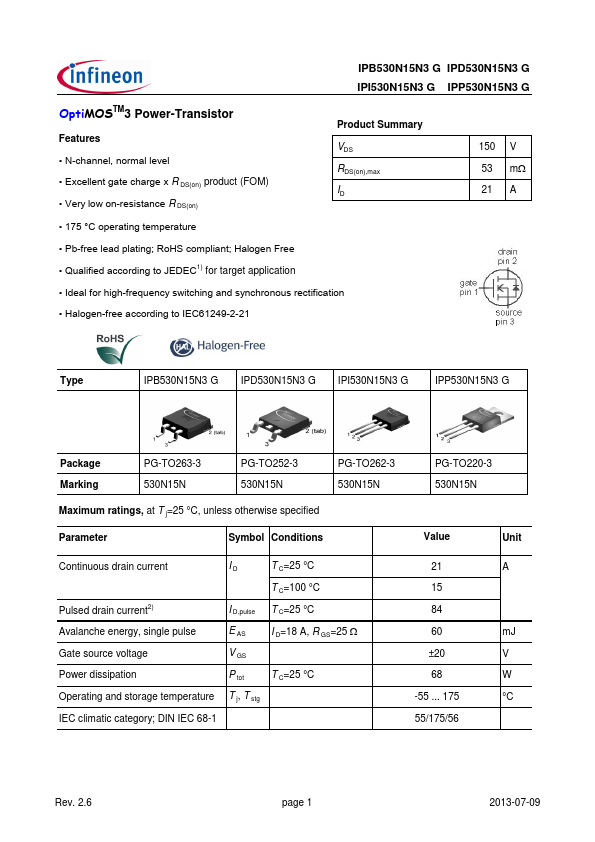
IPB530N15N3 G IPD530N15N3 G
IPI530N15N3 G IPP530N15N3 G
Parameter
Symbol Conditions
min.
Values
typ.
Unit
max.
Thermal characteristics
Thermal resistance, junction - case R thJC
-
Thermal resistance, junction -
ambient
R thJA minimal footprint
-
6 cm2 cooling area3)
-
-
2.2 K/W
-
62
-
40
Electrical characteristics, at T j=25 °C, unless otherwise specified
Static characteristics
Drain-source breakdown voltage
V (BR)DSS V GS=0 V, I D=1 mA
150
-
Gate threshold voltage
V GS(th) V DS=V GS, I D=35 µA
2
3
Zero gate voltage drain current
I DSS
V DS=120 V, V GS=0 V,
T j=25 °C
-
0.1
-V
4
1 µA
Gate-source leakage current
V DS=120 V, V GS=0 V,
T j=125 °C
-
I GSS
V GS=20 V, V DS=0 V
-
10
100
1
100 nA
Drain-source on-state resistance
R DS(on) V GS=10 V, I D=18 A
-
44
53 mW
Gate resistance
Transconductance
V GS=8 V, I D=9 A
-
44
53
RG
-
2.1
-W
g fs
|V DS|>2|I D|R DS(on)max,
I D=18 A
11
21
-S
1)J-STD20 and JESD22
2) See figure 3
3) Device on 40 mm x 40 mm x 1.5 mm epoxy PCB FR4 with 6 cm2 (one layer, 70 µm thick) copper area for drain
connection. PCB is vertical in still air.
Rev. 2.6
page 2
2013-07-09