IPB50R299CP Overview
Key Specifications
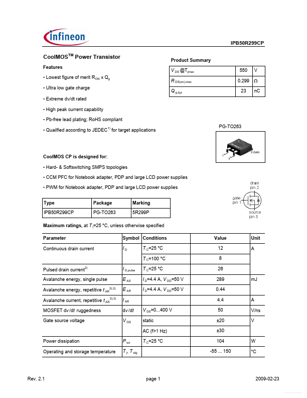
Package: TO-263-3
Mount Type: Surface Mount
Max Operating Temp: 150 °C
Min Operating Temp: -55 °C
Key Features
- Lowest figure of merit RON x Qg
- Ultra low gate charge
- Extreme dv/dt rated
- High peak current capability
- Pb-free lead plating; RoHS compliant