MJD47 Overview
Key Specifications
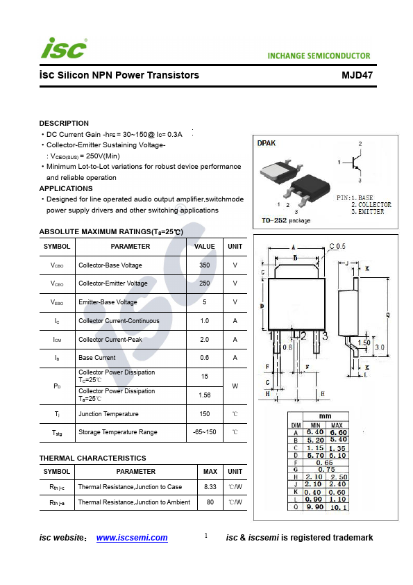
Package: DPAK
Pins: 3
Max Frequency: 2 MHz
Height: 2.38 mm
Description
DC Current Gain -hFE = 30~150@ IC= 0.3A - Collector-Emitter Sustaining Voltage- : VCEO(SUS) = 250V(Min) - Minimum Lot-to-Lot variations for robust device performance and reliable operation APPLICATIONS - Designed for line operated audio output amplifier,switchmode power supply drivers and other switching applications SYMBOL PARAMETER VALUE UNIT VCBO Collector-Base Voltage 350 V VCEO Collector-Emitter Voltage 250 V VEBO Emitter-Base Voltage 5 V IC Collector Current-Continuous 1.0 A ICM Collector Current-Peak 2.0 A IB Base Current Collector Power Dissipation TC=25℃ PD Collector Power Dissipation Ta=25℃ Tj Junction Temperature 0.6 A 15 W 1.56 150 ℃ Tstg Storage Temperature Range -65~150 ℃ SYMBOL PARAMETER Rth j-c Rth j-a MAX 8.33 80 UNIT ℃/W ℃/W isc website: 1 isc & iscsemi is registered trademark isc Silicon NPN Power Transistors INCHANGE Semiconductor MJD47 TC=25℃ unless otherwise specified SYMBOL PARAMETER CONDITIONS VCEO(SUS) Collector-Emitter Sustaining Voltage IC= 30mA; IB= 0 VCE(sat) Collector-Emitter Saturation Voltage IC= 1A; IB= 0.2A VBE(on) Base-Emitter On Voltage IC= 1A; VCE= 10V ICBO Collector Cutoff Current VCB= 350V; IE= 0 ICEO Collector Cutoff Current VCE= 150V; IB= 0 IEBO Emitter Cutoff Current VEB= 5V; IC= 0 hFE-1 DC Current Gain IC= 0.3A; VCE= 10V hFE-2 DC Current Gain IC= 1A; VCE= 10V fT Current-Gain-Bandwidth Product Pulse Test: PW≤300μs, Duty Cycle≤2.0% IC= 0.2A; VCE= 10V MIN MAX UNIT 250 V 1.0 V 1.5 V 0.1 mA 0.2 mA 1.0 mA 30 150 10 10 MHz NOTICE: ISC reserves the rights to make changes of the content herein the datasheet at any time without notification.