The following content is an automatically extracted verbatim text
from the original manufacturer datasheet and is provided for reference purposes only.
View original datasheet text
Preliminary Technical Information
TrenchMVTM
IXTA182N055T7
Power MOSFET
N-Channel Enhancement Mode Avalanche Rated
VDSS = ID25 =
RDS(on) ≤
55 182 5.0
V A mΩ
Symbol
VDSS VDGR VGSM ID25 ILRMS IDM IAR EAS dv/dt
PD TJ TJM Tstg TL TSOLD Weight
Test Conditions TJ = 25° C to 175° C TJ = 25° C to 175° C; RGS = 1 MΩ Transient TC = 25° C Package Current Limit, RMS TC = 25° C, pulse width limited by TJM TC = 25° C TC = 25° C IS ≤IDM, di/dt ≤100 A/µs, VDD ≤VDSS TJ ≤175° C, RG = 5 Ω TC = 25° C
1.6 mm (0.062 in.) from case for 10 s Plastic body for 10 seconds
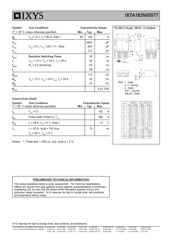
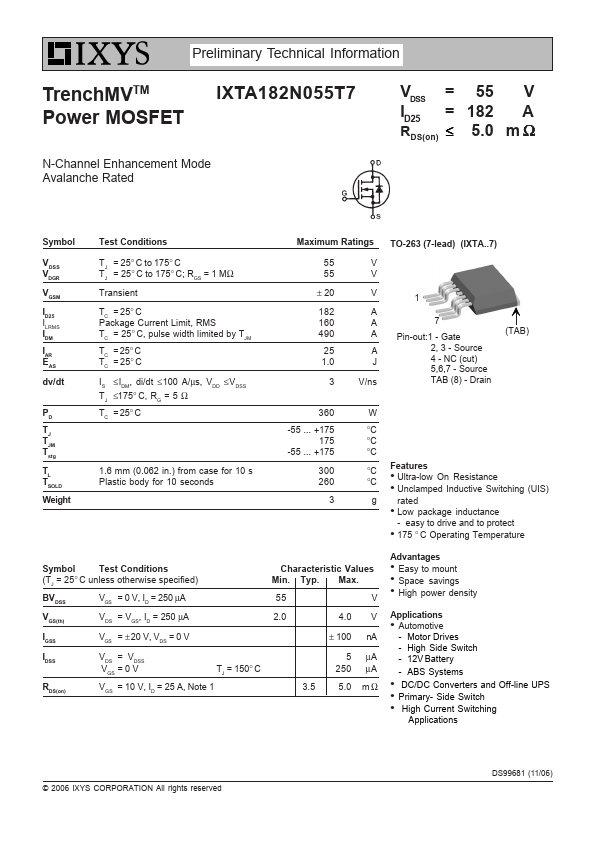
Maximum Ratings TO-263 (7-lead) (IXTA..7)
55 V 55 V
± 20
182 160 490
25 1.0
3
V
A A A
A J
V/ns
1
7
Pin-out:1 - Gate 2, 3 - Source 4 - NC (cut) 5,6,7 - Source TAB (8) - Drain
(TAB)
360
-55 ... +175 175
-55 ...
 IXTA182N055T7 Datasheet