Datasheet Details
| Part number | IS46LR32800G |
|---|---|
| Manufacturer | ISSI (now Infineon) |
| File Size | 1.40 MB |
| Description | 2M x 32Bits x 4Banks Mobile DDR SDRAM |
| Datasheet |
 IS46LR32800G Datasheet IS46LR32800G Datasheet
|
|
|
Download the IS46LR32800G datasheet PDF. This datasheet also covers the IS43LR32800G variant, as both devices belong to the same 2m x 32bits x 4banks mobile ddr sdram family and are provided as variant models within a single manufacturer datasheet.
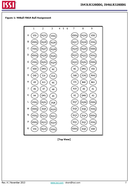
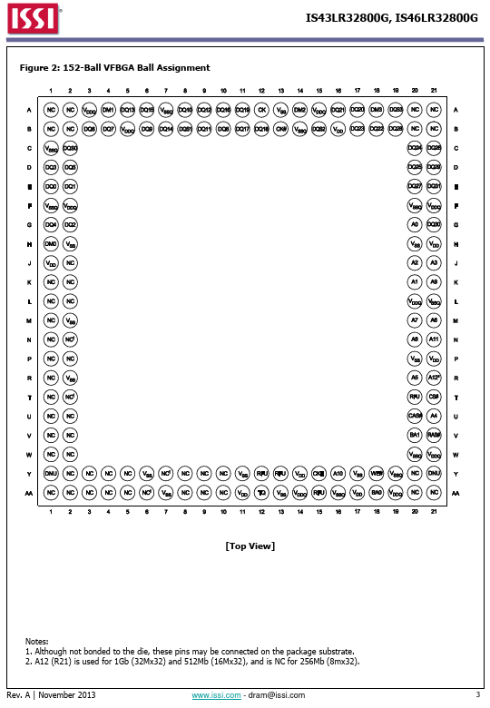
The IS43/46LR32800G is 268,435,456 bits CMOS Mobile Double Data Rate Synchronous DRAM organized as 4 banks of 2,097,152 words x 32 bits.
This product uses a double-data-rate architecture to achieve high-speed operation.
The Data Input/ Output signals are transmitted on a 32-bit bus.
| Part number | IS46LR32800G |
|---|---|
| Manufacturer | ISSI (now Infineon) |
| File Size | 1.40 MB |
| Description | 2M x 32Bits x 4Banks Mobile DDR SDRAM |
| Datasheet |
IS46LR32800G Datasheet
|
|
|
|
| Part Number | Description | Manufacturer |
|---|---|---|
| IS46R16160F | 256Mb DDR SDRAM | Integrated Silicon Solution |
| IS46R16320D | 16Mx32 32Mx16 64Mx8 512Mb DDR SDRAM | Integrated Silicon Solution |
| IS46R16320E | 512Mb DDR SDRAM | Integrated Silicon Solution |
| IS46R16800E | 128Mb DDR SDRAM | Integrated Silicon Solution |
| IS46R32160D | 16Mx32 32Mx16 64Mx8 512Mb DDR SDRAM | Integrated Silicon Solution |
| Part Number | Description |
|---|---|
| IS46LR32800F | 2M x 32Bits x 4Banks Mobile DDR SDRAM |
| IS46LR32800H | 2M x 32Bits x 4Banks Mobile DDR SDRAM |
| IS46LR32100C | 512K x 32Bits x 2Banks Mobile DDR SDRAM |
| IS46LR32100D | 512K x 32Bits x 2Banks Mobile DDR SDRAM |
| IS46LR32160B | 4M x 32Bits x 4Banks Mobile DDR SDRAM |
The following content is an automatically extracted verbatim text from the original manufacturer datasheet and is provided for reference purposes only.