Ultra low gate charge
High peak current capability
Improved transconductance
ABSOLUTE MAXIMUM RATINGS(Ta=25℃)
SYMBOL
PARAMETER
VALUE
VDSS
Drain-Source Voltage
600
VGS
Gate-Source Voltage
±20
ID
Drain Current-Continuous
7.3
IDM
Drain Current-Single Pulsed
21.9
PD
Features
Static drain-source on-resistance:
RDS(on) ≤0.6Ω.
Enhancement mode.
Fast Switching Speed.
100% avalanche tested.
Minimum Lot-to-Lot variations for robust device
performance and reliable operation.
The following content is an automatically extracted verbatim text
from the original manufacturer datasheet and is provided for reference purposes only.
View original datasheet text
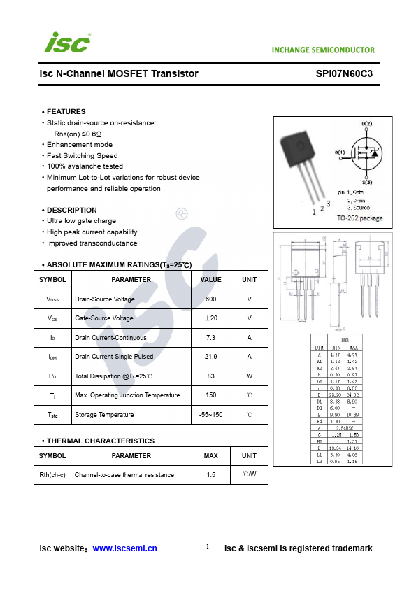
isc N-Channel MOSFET Transistor
·FEATURES ·Static drain-source on-resistance:
RDS(on) ≤0.6Ω ·Enhancement mode ·Fast Switching Speed ·100% avalanche tested ·Minimum Lot-to-Lot variations for robust device
performance and reliable operation
·DESCRIPTION ·Ultra low gate charge ·High peak current capability ·Improved transconductance
·ABSOLUTE MAXIMUM RATINGS(Ta=25℃)
SYMBOL
PARAMETER
VALUE
VDSS
Drain-Source Voltage
600
VGS
Gate-Source Voltage
±20
ID
Drain Current-Continuous
7.3
IDM
Drain Current-Single Pulsed
21.9
PD
Total Dissipation @TC=25℃
83
Tj
Max. Operating Junction Temperature
150
Tstg
Storage Temperature
-55~150
UNIT V V A A W ℃ ℃
·THERMAL CHARACTERISTICS
SYMBOL
PARAMETER
Rth(ch-c) Channel-to-case thermal resistance
MAX 1.
 SPI07N60C3 Datasheet