Datasheet4U Logo Datasheet4U.com

ICS854S202I - Differential-to-LVDS Multiplexer

Description

The ICS854S202I is a 12:2 Differential-to-LVDS Clock Multiplexer which can operate up to 3GHz.

The ICS854S202I has twelve selectable differential clock inputs, any of which can be independently routed to either of the two LVDS outputs.

The CLKx, nCLKx input pairs can accept LVPECL, LVDS, CML levels.

Features

  • Two differential 3.3V LVDS clock outputs.
  • Twelve selectable differential clock inputs.
  • CLKx, nCLKx pairs can accept the following differential input levels: LVPECL, LVDS, CML.
  • Maximum output frequency: 3GHz.
  • Propagation delay: 1.1ns (maximum).
  • Input skew: 100ps (maximum).
  • Output skew: 50ps (maximum).
  • Part-to-part skew: 250ps (maximum).
  • Additive phase jitter, RMS (12kHz.
  • 20MHz): 0.16ps (typical).
  • F.

📥 Download Datasheet

Datasheet Details

Part number ICS854S202I
Manufacturer IDT
File Size 419.50 KB
Description Differential-to-LVDS Multiplexer
Datasheet download datasheet ICS854S202I Datasheet

Full PDF Text Transcription (Reference)

The following content is an automatically extracted verbatim text from the original manufacturer datasheet and is provided for reference purposes only.

View original datasheet text
12:2, Differential-to-LVDS Multiplexer
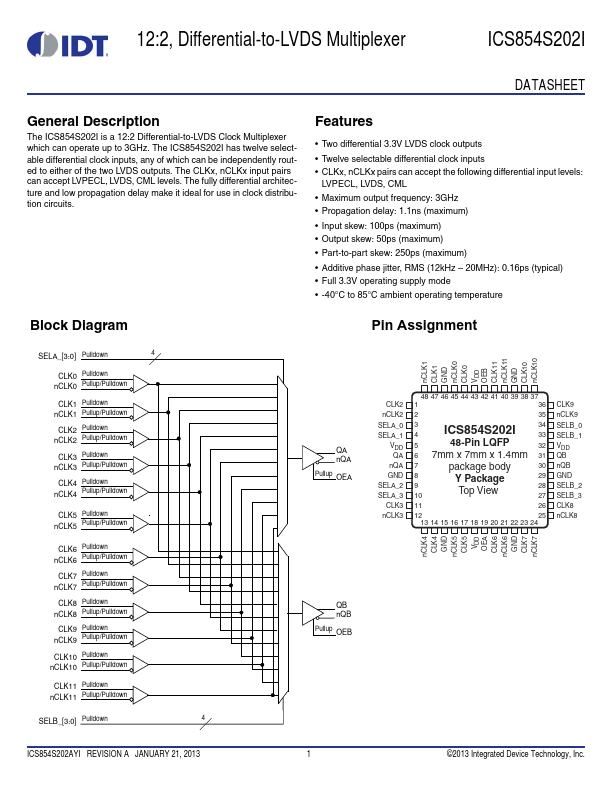
 ICS854S202I DATASHEET General Description The ICS854S202I is a 12:2 Differential-to-LVDS Clock Multiplexer which can operate up to 3GHz. The ICS854S202I has twelve selectable differential clock inputs, any of which can be independently routed to either of the two LVDS outputs. The CLKx, nCLKx input pairs can accept LVPECL, LVDS, CML levels. The fully differential architecture and low propagation delay make it ideal for use in clock distribution circuits. Features • Two differential 3.3V LVDS clock outputs • Twelve selectable differential clock inputs • CLKx, nCLKx pairs can accept the following differential input levels: LVPECL, LVDS, CML • Maximum output frequency: 3GHz • Propagation delay: 1.
Published: |