Click to expand full text
PCI Express Jitter Attenuator
9DB306
Data Sheet
GENERAL DESCRIPTION
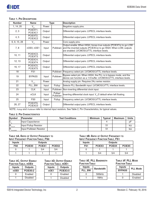
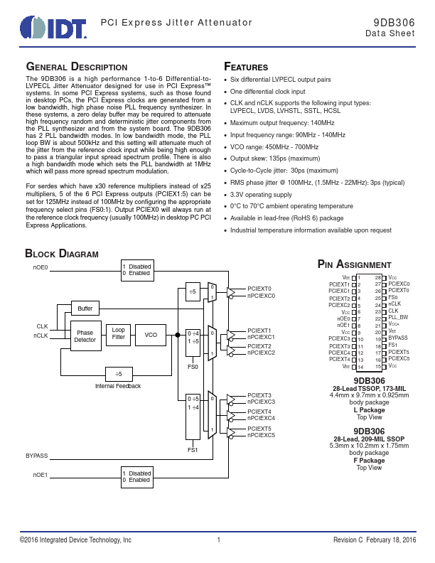
The 9DB306 is a high performance 1-to-6 Differential-toLVPECL Jitter Attenuator designed for use in PCI Express™ systems. In some PCI Express systems, such as those found in desktop PCs, the PCI Express clocks are generated from a low bandwidth, high phase noise PLL frequency synthesizer. In these systems, a zero delay buffer may be required to attenuate high frequency random and deterministic jitter components from the PLL synthesizer and from the system board. The 9DB306 has 2 PLL bandwidth modes. In low bandwidth mode, the PLL loop BW is about 500kHz and this setting will attenuate much of the jitter from the reference clock input while being high enough to pass a triangular input spread spectrum profile.
 9DB306 Datasheet