8V19N880 Datasheet Text
FemtoClock® NG Jitter Attenuator and Clock Synthesizer
8V19N880
Short-Form Datasheet
Description
The 8V19N880 is a fully integrated FemtoClock® NG jitter attenuator and clock synthesizer designed as a high-performance clock solution for conditioning and frequency/phase management of wireless base station radio equipment boards. The device is optimized to deliver excellent phase noise performance as required in GSM, WCDMA, LTE, LTE-A, and 5G radio board implementations. The device supports JESD204B (subclass 0 and 1) and JESD204C.
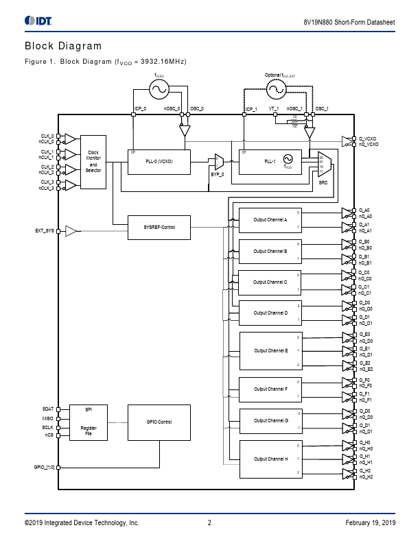
The 8V19N880 has a two-stage PLL architecture that supports both jitter attenuation and frequency multiplication. The first stage PLL is the jitter attenuator and uses an external VCXO for best possible phase noise characteristics. The second stage PLL locks on the PLL-0 output signal and synthesizes the target frequency. The second stage PLL can use the internal or an external high-frequency VCO.
The 8V19N880 supports the clock generation of high-frequency clocks from the selected VCO and low-frequency synchronization signals (SYSREF). SYSREF signals are internally synchronized to the clock signals. Delay functions exist for achieving alignment and controlled phase delay between system reference and clock signals and to align/delay individual output signals. The four redundant inputs are monitored for activity. Four selectable clock switching modes are provided to handle clock input failure scenarios. Auto-lock, individually programmable output frequency dividers, and phase adjustment capabilities are added for additional flexibility.
The 8V19N880 is configured through a 3/4-wire SPI interface and reports lock and signal loss status in internal registers and via the GPIO[1:0] outputs. Internal status bit changes can also be reported via a...