5PB1110NDGI
Overview
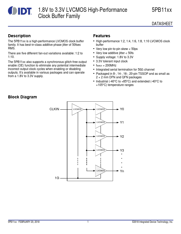
The 5PB11xx is a high-performance LVCMOS clock buffer family. It has best-in-class additive phase jitter of 50fsec RMS.
- High-performance 1:2, 1:4, 1:6, 1:8, 1:10 LVCMOS clock buffer
- Very low pin-to-pin skew < 50ps
- Very low additive jitter < 50fs
- Supply voltage: 1.8V to 3.3V
- 3.3V tolerant input clock
- fMAX = 200MHz
- Integrated serial termination for 50 channel
- Packaged in 8-, 14-, 16-, 20-pin TSSOP and as small as 2 × 2 mm DFN and QFN packages
- Industrial (-40°C to +85°C) and extended (-40°C to +105°C) temperature ranges