Datasheet4U Logo Datasheet4U.com

HYMD232G726BLF8-J - Registered DDR SDRAM DIMM

Download the HYMD232G726BLF8-J datasheet PDF. This datasheet also covers the HYMD232G726BF8-J variant, as both devices belong to the same registered ddr sdram dimm family and are provided as variant models within a single manufacturer datasheet.
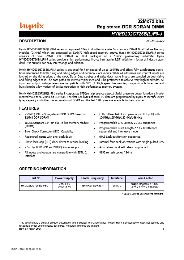
Description

Hynix HYMD232G726B(L)F8-J series is registered 184-pin double data rate Synchronous DRAM Dual In-Line Memory Modules (DIMMs) which are organized as 32Mx72 high-speed memory arrays.

Features

  • 256MB (32Mx72) Registered DDR DIMM based on 32Mx8 DDR SDRAM JEDEC Standard 184-pin dual in-line memory module (DIMM) Error Check Correction (ECC) Capability Registered inputs with one-clock delay Phase-lock loop (PLL) clock driver to reduce loading 2.5V +/- 0.2V VDD and VDDQ Power supply All inputs and outputs are compatible with SSTL_2 interface.
  • Fully diffe.

📥 Download Datasheet

Note: The manufacturer provides a single datasheet file (HYMD232G726BF8-J_HynixSemiconductor.pdf) that lists specifications for multiple related part numbers.

Full PDF Text Transcription (Reference)

The following content is an automatically extracted verbatim text from the original manufacturer datasheet and is provided for reference purposes only.

View original datasheet text
32Mx72 bits Registered DDR SDRAM DIMM HYMD232G726B(L)F8-J DESCRIPTION www.DataSheet4U.com Preliminary Hynix HYMD232G726B(L)F8-J series is registered 184-pin double data rate Synchronous DRAM Dual In-Line Memory Modules (DIMMs) which are organized as 32Mx72 high-speed memory arrays. Hynix HYMD232G726B(L)F8-J series consists of nine 32Mx8 DDR SDRAM in FBGA packages on a 184pin glass-epoxy substrate. Hynix HYMD232G726B(L)F8-J series provide a high performance 8-byte interface in 5.25" width form factor of industry standard. It is suitable for easy interchange and addition. Hynix HYMD232G726B(L)F8-J series is designed for high speed of up to 166MHz and offers fully synchronous operations referenced to both rising and falling edges of differential clock inputs.
Published: |