Silicon N-Channel Power MOSFET
CS14N10 A3
○R
General Description
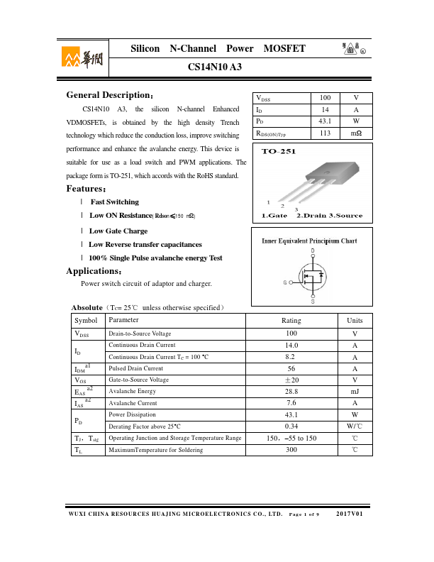
:
CS14N10 A3, the silicon N-channel Enhanced
VDMOSFETs, is obtained by the high density Trench
technology which reduce the conduction loss, improve switching
VDSS
ID
PD
RDS(ON)Typ
performance and enhance the avalanche energy. This device is
suitable for use as a load switch and PWM applications. The
package form is TO-251, which accords with the RoHS standard.
Features:
l Fast Switching
l Low ON Resistance(Rdson≤150 mΩ)
l Low Gate Charge
l Low Reverse transfer capacitances
l 100% Single Pulse avalanche energy Test
Applications:
Power switch circuit of adaptor and charger.
100 V
14 A
43.1 W
113 mΩ
Absolute(TC= 25℃ unless otherwise specified)
Symbol Parameter
VDSS
ID
IDMa1
VGS
EAS a2
IAS a2
PD
TJ,Tstg
TL
Drain-to-Source Voltage
Continuous Drain Current
Continuous Drain Current TC = 100 °C
Pulsed Drain Current
Gate-to-Source Voltage
Avalanche Energy
Avalanche Current
Power Dissipation
Derating Factor above 25°C
Operating Junction and Storage Temperature Range
MaximumTemperature for Soldering
Rating
100
14.0
8.2
56
±20
28.8
7.6
43.1
0.34
150,–55 to 150
300
Units
V
A
A
A
V
mJ
A
W
W/℃
℃
℃
WUXI CHI NA RESOURCES HUAJ I NG M I CROELECTRONI CS C O. , LTD. Pag e 1 of 9
2017V01