2SJ317
Overview
- Very low on-resistance
- High speed switching
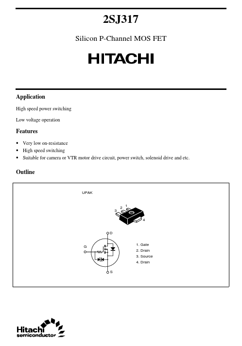
- Suitable for camera or VTR motor drive circuit, power switch, solenoid drive and etc. Outline
| Part | 2SJ317 |
|---|---|
| Description | P-Channel MOSFET |
| Category | MOSFET |
| Manufacturer | Hitachi Semiconductor |
| Size | 38.78 KB |
| Part Number | Manufacturer | Description |
|---|---|---|
| 2SJ316 | SANYO | P-Channel MOSFET |
| 2SJ313 | Toshiba | P-Channel MOSFET |
| 2SJ319S | Kexin Semiconductor | P-Channel MOSFET |
| 2SJ312 | Toshiba | P-Channel MOSFET |
| 2SJ315 | Toshiba | P-Channel MOSFET |