Datasheet4U Logo Datasheet4U.com

GD25Q20 - Dual and Quad SPI Flash

Download the GD25Q20 datasheet PDF (GD25Q40 included). The manufacturer datasheet provides complete specifications, pinout details, electrical characteristics, and typical applications for dual and quad spi flash.

Description

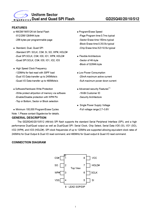
I/O2 (WP#), and I/O3 (HOLD#).

Features

  • 4M/2M/1M/512K-bit Serial Flash -512/256/128/64K-byte -256 bytes per programmable page.
  • Standard, Dual, Quad SPI -Standard SPI: SCLK, CS#, SI, SO, WP#, HOLD# -Dual SPI:SCLK, CS#, IO0, IO1, WP#, HOLD# -Quad SPI:SCLK, CS#, IO0, IO1, IO2, IO3.
  • High Speed Clock Frequency -120MHz for fast read with 30PF load -Dual I/O Data transfer up to 240Mbits/s -Quad I/O Data transfer up to 480Mbits/s.
  • Program/Erase Speed -Page Program time:0.7ms typical -Sector Erase time:150ms typical -Bloc.

📥 Download Datasheet

Note: The manufacturer provides a single datasheet file (GD25Q40-GigaDevice.pdf) that lists specifications for multiple related part numbers.
Other Datasheets by GigaDevice

Full PDF Text Transcription

Click to expand full text
Uniform Sector Dual and Quad SPI Flash GD25Q40/20/10/512 FEATURES ◆ 4M/2M/1M/512K-bit Serial Flash -512/256/128/64K-byte -256 bytes per programmable page ◆ Standard, Dual, Quad SPI -Standard SPI: SCLK, CS#, SI, SO, WP#, HOLD# -Dual SPI:SCLK, CS#, IO0, IO1, WP#, HOLD# -Quad SPI:SCLK, CS#, IO0, IO1, IO2, IO3 ◆ High Speed Clock Frequency -120MHz for fast read with 30PF load -Dual I/O Data transfer up to 240Mbits/s -Quad I/O Data transfer up to 480Mbits/s ◆ Program/Erase Speed -Page Program time:0.7ms typical -Sector Erase time:150ms typical -Block Erase time:0.3.5s typical -Chip Erase time:321.
Published: |