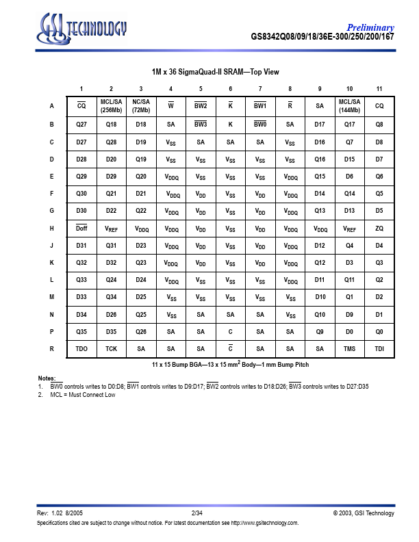
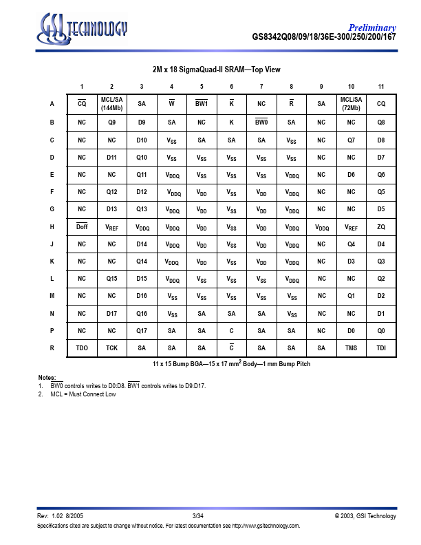
GS8342Q08E-300 - 36Mb SigmaQuad-II Burst of 2 SRAM
GSI Technology
Description
Table
Symbol
SA NC R W
BW
Description
Synchronous Address Inputs No Connect
Synchronous Read Synchronous Write
Synchronous Byte Write
BW0
BW3
Synchronous Byte Writes
NW0
NW1
Nybble Write Control Pin
K Input Clock
K Input Clock
C Output Clock
C Output Clock
TMS Test Mode Sel
The following content is an automatically extracted verbatim text
from the original manufacturer datasheet and is provided for reference purposes only.
View original datasheet text
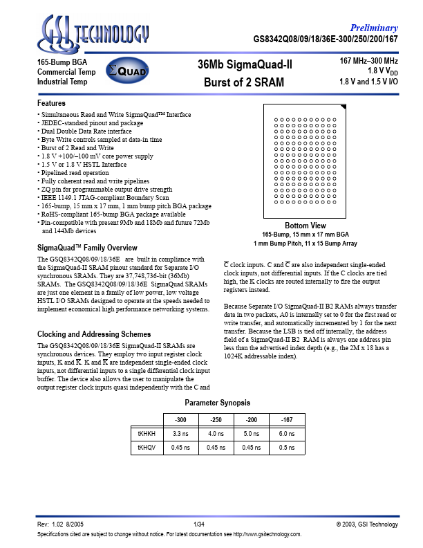
Preliminary GS8342Q08/09/18/36E-300/250/200/167
165-Bump BGA Commercial Temp Industrial Temp
36Mb SigmaQuad-II Burst of 2 SRAM
167 MHz–300 MHz 1.8 V VDD
1.8 V and 1.5 V I/O
Features
• Simultaneous Read and Write SigmaQuad™ Interface • JEDEC-standard pinout and package • Dual Double Data Rate interface • Byte Write controls sampled at data-in time • Burst of 2 Read and Write • 1.8 V +100/–100 mV core power supply • 1.5 V or 1.8 V HSTL Interface • Pipelined read operation • Fully coherent read and write pipelines • ZQ pin for programmable output drive strength • IEEE 1149.
 GS8342Q08E-300 Datasheet