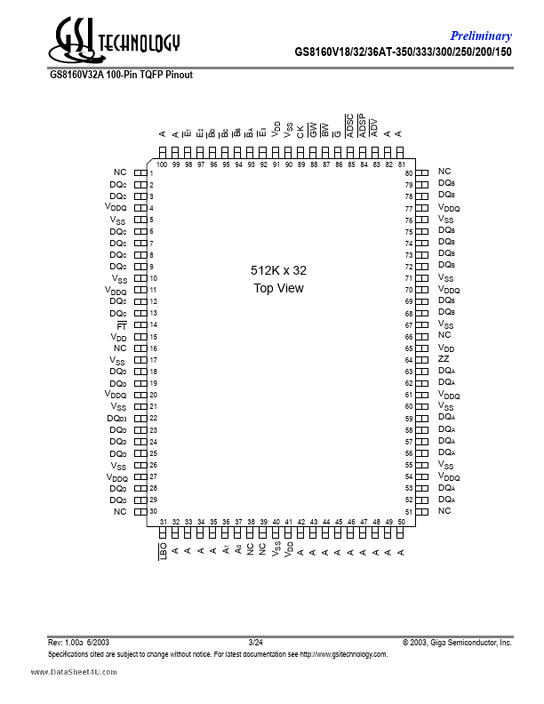
Datasheet4U Logo Datasheet4U.com

GS8160V32AT - 1M x 18 512K x 32 512K x 36 18Mb Sync Burst SRAMs

Download the GS8160V32AT datasheet PDF. This datasheet also covers the GS8160V18AT variant, as both devices belong to the same 1m x 18 512k x 32 512k x 36 18mb sync burst srams family and are provided as variant models within a single manufacturer datasheet.

General Description

The GS8160V18/32/36AT is an 18,874,368-bit (16,777,216-bit for x32 version) high performance synchronous SRAM with a 2-bit burst address counter.

Key Features

  • 1M x 18, 512K x 32, 512K x 36 18Mb Sync Burst SRAMs 350 MHz.
  • 150 MHz 1.8 V VDD 1.8 V I/O.
  • FT pin for user-configurable flow through or pipeline operation.
  • Single Cycle Deselect (SCD) operation.
  • 1.8 V +10%/.
  • 10% core power supply.
  • 1.8 V I/O supply.
  • LBO pin for Linear or Interleaved Burst mode.
  • Internal input resistors on mode pins allow floating mode pins.
  • Default to Interleaved Pipeline mode.
  • Byte Write (BW).

📥 Download Datasheet

Note: The manufacturer provides a single datasheet file (GS8160V18AT_GSITechnology.pdf) that lists specifications for multiple related part numbers.

Datasheet Details

Part number GS8160V32AT
Manufacturer GSI Technology
File Size 528.89 KB
Description 1M x 18 512K x 32 512K x 36 18Mb Sync Burst SRAMs
Datasheet download datasheet GS8160V32AT Datasheet

Full PDF Text Transcription (Reference)

The following content is an automatically extracted verbatim text from the original manufacturer datasheet and is provided for reference purposes only.

View original datasheet text
Preliminary www.DataSheet4U.com GS8160V18/32/36AT-350/333/300/250/200/150 100-Pin TQFP Commercial Temp Industrial Temp Features 1M x 18, 512K x 32, 512K x 36 18Mb Sync Burst SRAMs 350 MHz–150 MHz 1.8 V VDD 1.8 V I/O • FT pin for user-configurable flow through or pipeline operation • Single Cycle Deselect (SCD) operation • 1.8 V +10%/–10% core power supply • 1.8 V I/O supply • LBO pin for Linear or Interleaved Burst mode • Internal input resistors on mode pins allow floating mode pins • Default to Interleaved Pipeline mode • Byte Write (BW) and/or Global Write (GW) operation • Internal self-timed write cycle • Automatic power-down for portable applications • JEDEC-standard 100-lead TQFP package cycles can be initiated with either ADSP or ADSC inputs.