logo

GS8150V18AB-250 Datasheet, GSI Technology

GS8150V18AB-250 sram equivalent, 1m x 18/ 512k x 36 18mb register-register late write sram.

GS8150V18AB-250 Avg. rating / M : 1.0 rating-11

datasheet Download (Size : 842.40KB)

GS8150V18AB-250 Datasheet
GS8150V18AB-250 Avg. rating / M : 1.0 rating-11

datasheet Download (Size : 842.40KB)

GS8150V18AB-250 Datasheet

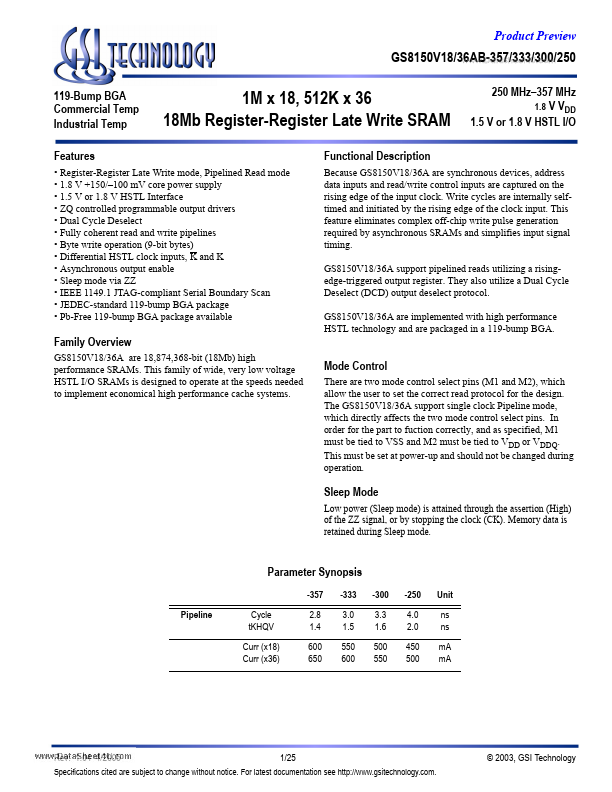
Features and benefits


* Register-Register Late Write mode, Pipelined Read mode
* 1.8 V +150/
  –100 mV core power supply
* 1.5 V or 1.8 V HSTL Interface
* ZQ contr.

Application

and in Flow Through mode NBT SRAMs. Byte Write Control The Byte Write Enable inputs (Bx) determine which bytes will be w.

Description

250 MHz
  –357 MHz 1.8 V VDD 1.5 V or 1.8 V HSTL I/O Because GS8150V18/36A are synchronous devices, address data inputs and read/write control inputs are captured on the rising edge of the input clock. Write cycles are internally selft.

Image gallery

GS8150V18AB-250 Page 1 GS8150V18AB-250 Page 2 GS8150V18AB-250 Page 3

TAGS

GS8150V18AB-250
512K
18Mb
Register-Register
Late
Write
SRAM
GSI Technology

Manufacturer


GSI Technology

Related datasheet

GS8150V18AB-300

GS8150V18AB-333

GS8150V18AB-357

GS8150V36AB-250

GS8150V36AB-300

GS8150V36AB-333

GS8150V36AB-357

GS815018AB-250

GS815018AB-300

GS815018AB-333

GS815018AB-357

GS815036AB-250

GS815036AB-300

Since 2006. D4U Semicon.   |   Contact Us   |   Privacy Policy   |   Purchase of parts