GS81302S18GE
GS81302S18GE is 144Mb SigmaSIO DDR -II Burst of 2 SRAM manufactured by GSI Technology.
- Part of the GS81302S08E-375 comparator family.
- Part of the GS81302S08E-375 comparator family.
GS81302S08/09/18/36E-375/350/333/300/250
165-Bump BGA mercial Temp Industrial Temp
144Mb Sigma SIOTM DDR -II Burst of 2 SRAM
375 MHz- 250 MHz 1.8 V VDD
1.8 V and 1.5 V I/O
Features
- Simultaneous Read and Write Sigma SIO™ Interface
- JEDEC-standard pinout and package
- Dual Double Data Rate interface
- Byte Write controls sampled at data-in time
- DLL circuitry for wide output data valid window and future frequency scaling
- Burst of 2 Read and Write
- 1.8 V +100/- 100 m V core power supply
- 1.5 V or 1.8 V HSTL Interface
- Pipelined read operation
- Fully coherent read and write pipelines
- ZQ mode pin for programmable output drive strength
- IEEE 1149.1 JTAG-pliant Boundary Scan
- 165-bump, 15 mm x 17 mm, 1 mm bump pitch BGA package
- Ro HS-pliant 165-bump BGA package available
Sigma SIO™ Family Overview
GS81302S08/09/18/36 are built in pliance with the Sigma SIO DDR-II SRAM pinout standard for Separate I/O synchronous SRAMs. They are 150,994,944-bit (144Mb) SRAMs. These are the first in a family of wide, very low voltage HSTL I/O SRAMs designed to operate at the speeds needed to implement economical high performance networking systems.
Clocking and Addressing Schemes
A Burst of 2 Sigma SIO DDR-II SRAM is a synchronous device. It employs dual input register clock inputs, K and K. The device also allows the user to manipulate the output register clock input quasi independently with dual output register clock inputs, C and C. If the C clocks are tied high, the
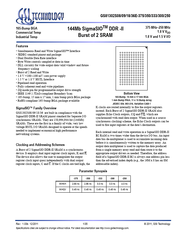
Bottom View
165-Bump, 15 mm x 17 mm BGA 1 mm Bump Pitch, 11 x 15 Bump Array
JEDEC Std. MO-216, Variation CAB-1
K clocks are routed internally to fire the output registers instead. Each Burst of 2 Sigma SIO DDR-II SRAM also supplies Echo Clock outputs, CQ and CQ, which are synchronized with read data output. When used in a source synchronous clocking scheme, the Echo Clock outputs can be used to fire input registers at the data’s destination.
Each internal read and write operation in a Sigma SIO DDR-II...