Download the GS81302S09GE datasheet PDF.
This datasheet also covers the GS81302S08E-375 variant, as both devices belong to the same 144mb sigmasio ddr -ii burst of 2 sram family and are provided as variant models within a single manufacturer datasheet.
Description
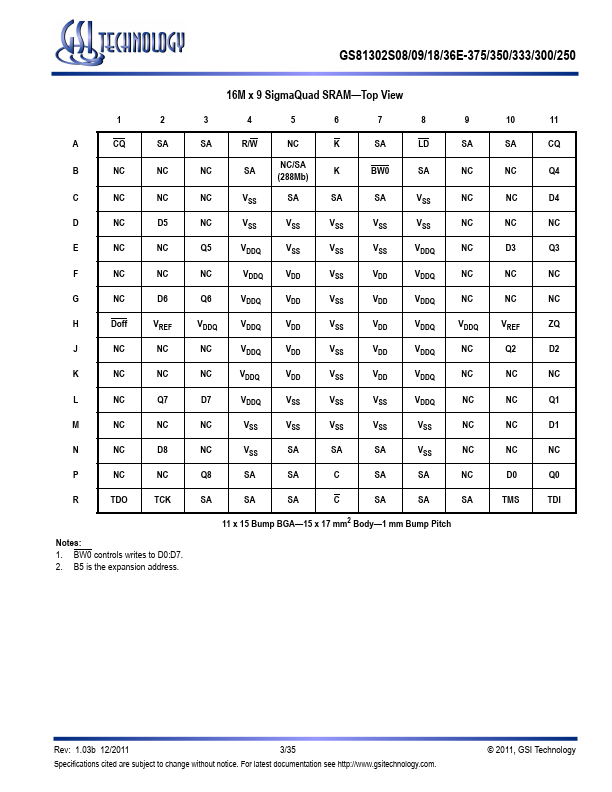
Table
Symbol
Description
Type Comments
SA
Synchronous Address Inputs
Input
R/W
Read/Write Contol Pin
Input Write Active Low; Read Active High
NW0
NW1
Synchronous Nybble Writes
Input
Active Low x08 Version
BW0
BW1
Synchronous Byte Writes
Input
Active Low x18
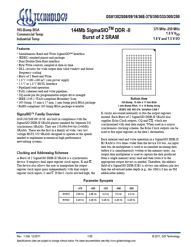
Features
- Simultaneous Read and Write SigmaSIO™ Interface.
- JEDEC-standard pinout and package.
- Dual Double Data Rate interface.
- Byte Write controls sampled at data-in time.
- DLL circuitry for wide output data valid window and future
frequency scaling.
- Burst of 2 Read and Write.
- 1.8 V +100/.
- 100 mV core power supply.
- 1.5 V or 1.8 V HSTL Interface.
- Pipelined read operation.
- Fully coherent read and write pipelines.
 GS81302S09GE Datasheet