GOFORD
630A
Electrical Characteristics TC=25℃ unless otherwise specified
Symbol
Parameter
Off Characteristic
V(BR)DSS
△V(BR)DSS
/△TJ
Drain-Source Breakdown Voltage
Breakdown Voltage Temperature
Coefficient
IDSS Zero Gate Voltage Drain Current
IGSS Gate to Body Leakage Current
On Characteristics
VGS(th)
Gate Threshold Voltage note4
RDS(on)
Static Drain-Source On-Resistance
gFS Forward Transconductance
Dynamic Characteristics
Ciss Input Capacitance
Coss Output Capacitance
Crss Reverse Transfer Capacitance
Qg Total Gate Charge
Qgs Gate-Source Charge
Qgd Gate-Drain(“Miller”) Charge
Test Condition
VGS = 0V,ID = 250µA
Reference to 25℃,
ID = 250µA
VDS = 200V, VGS = 0V
VDS = 160V, TC = 125℃
VDS = 0V, VGS = ±30V
VDS = VGS, ID = 250µA
VGS =10V, ID = 4.5A
VDS =30V, ID = 4.5A
VDS = 25V, VGS = 0V,
f = 1.0MHz
VDD = 160V, ID = 9A,
VGS = 10V
Switching Characteristics
td(on)
Turn-On Delay Time
tr Turn-On Rise Time
td(off)
Turn-Off Delay Time
VDD = 100V, ID = 9A,
RG = 10Ω, VGS = 10V
tf Turn-Off Fall Time
Drain-Source Diode Characteristics and Maximum Ratings
IS Maximum Continuous Drain to Source Diode Forward Current
ISM Maximum Pulsed Drain to Source Diode Forward Current
VSD Drain to Source Diode Forward Voltage VGS = 0V, IS = 9A
trr Reverse Recovery Time
Qrr Reverse Recovery Charge
VGS = 0V, IF = 9A,
di/dt =100A/µs
Notes:
1. Repetitive Rating: 
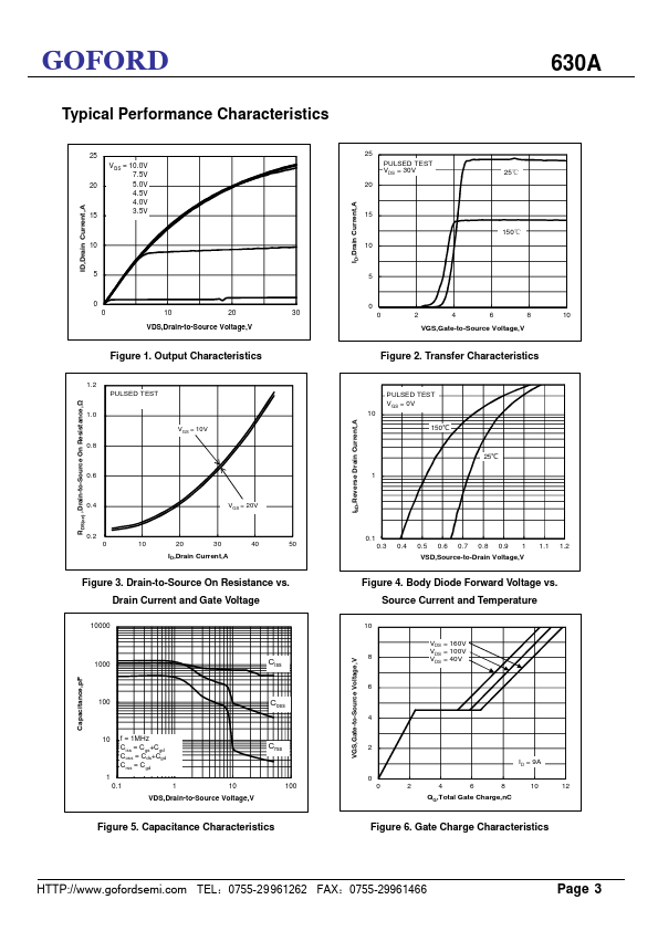
Pulse width limited by maximum junction temperature
2. L = 10mH, IAS = 8A, VDD = 50V, RG = 25Ω, Starting TJ = 25°C
3. ISD ≤ 9A, di/dt ≤ 200A/µs, VDD ≤ BVDSS, Starting TJ = 25°C
4. Pulse width ≤ 300µs; duty cycle ≤ 2%.
Min. Typ. Max.
200 -
-
- 0.25 -
--1
- - 10
- - ±100
1 1.8 2.5
- 0.21 0.25
- 9.2
-
- 509
- 51.5
- 3.2
- 11.8
- 2.36
- 3.98
-
-
-
-
-
-
- 10.33
- 10.7
- 29.1
- 11.1
-
-
-
-
-- 9
- - 36
- - 1.4
- 201 -
- 663 -
Units
V
V/℃
µA
µA
nA
V
Ω
S
pF
pF
pF
nC
nC
nC
ns
ns
ns
ns
A
A
V
ns
nC
HTTP://www.gofordsemi.com TEL:0755-29961262 FAX:0755-29961466
Page 2