1404TR
1404TR is N-Channel MOSFETS manufactured by GFD.
DESCRIPTION
The OGFD 1404TR uses advanced trench technology and design to provide excellent RDS(ON) with low gate charge. It can be used in a wide variety of applications.
Features
:
- High density cell design for ultra low Rdson.
- Fully characterized avalanche voltage and current.
- Good stability and uniformity with high EAS.
- Excellent package for good heat dissipation.
- Special process technology for high ESD capability.
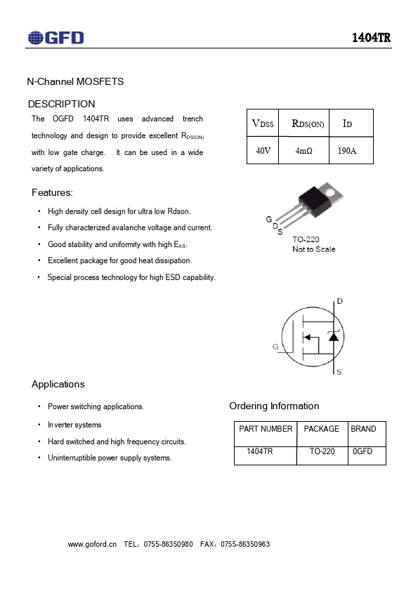
VDSS RDS(ON) ID
40V 4mΩ 190A
Applications
- Power switching applications.
- In verter systems
- Hard switched and high frequency circuits.
- Uninterruptible power supply systems.
Ordering Information
PART NUMBER PACKAGE BRAND
TO-220 0GFD
.goford.cn TEL:0755-86350980 FAX:0755-86350963
Absolute Maximum Ratings (TC=25℃, unless otherwise noted)
Symbol
Parameter
Units
VDSS ID IDM
VGS EAS dv/dt TJ and TSTG
Drain-to-Source Voltage Continuous Drain Current Pulsed Drain...