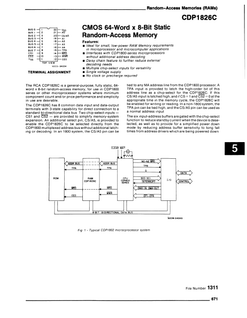
••Random-A~_M.morl (RAM.) ______________________________________~
CDP1828C
Two memory control signals, MRD and MWR, are provided
for reading from and writing to the CDP1826C. The logic is
designed so that MWR overrides MRD, allowing the chip to
be controlled from a Single R/iNline
For such an Interface, the MRD line can be tied to Vss, with
the MWR line connected to R/iN.
A CHIP ENABLE OUTPUT is provided for daisy-chaining to
additional memories or 1/0 devices. This output is high
whenever the chip-select function selects the CDP1826C,
which deselects any other chip which has its CS input
connected to the CDP1826C CEO output. The connected
£!!!£.is selected when the CDP1826C is de-selected and the
MRD input is low. Thus, the CEO is only active for a read
cycle and can be set up so that a CEO of another device can
feed the MRi5 of the CDP1826C, which in turn selects a third
chip in the daisy chain.
The CDP1826C has a recommended operating voltage of
4.5 to 5.5 V and is supplied in 22-lead hermetic dual-in-line
side-brazed ceramic packages (D suffix), in 22-lead dual-
in-line plastic packages (E suffix). The CDP1826C is also
available in chip form (H suffiX).
MAXIMUM RATINGS. Absolute-MaxImum Values:
DC SUPPLY-VOLTAGE RANGE, (Voo)
(Voltages referenced to Vss Terminal) .............................................................................. -0.5 to +7 V
INPUT VOLTAGE RANGE, ALL INPUTS .........................................................................-0.5 to Voo +0.5 V
DC INPUT CURRENT, ANY ONE INPUT ..................................................................................±10 rnA
POWER DISSIPATION PER PACKAGE (Po)
For TA= -40 to + 60° C (PACKAGE TYPE E) ............................................................................ 500 mW
For TA= + 60 to + 85° C (PACKAGE TYPE E) ............................................. Derate Linearly at 12 mW/O C to 200 mW
For TA = -55 to + 100°C (PACKAGE TYPE D) ........................................................................... 500 mW
For TA= + 100 to + 125° C (PACKAGE TYPE D) .......................................... Derate Linearly at 12 mW/o C to 200 mW
DEVICE DISSIPATION PER OUTPUT TRANSISTOR
For TA = FULL PACKAGE-TEMPERATURE RANGE (All Package Types) .................................................. 100 mW
OPERATING-TEMPERATURE RANGE (TA)
PACKAGE TYPE D .............................................................................................. -55 to +125°C
PACKAGE TYPE E ......................................................................................••.•.•... -40 to +85°C
STORAGE TEMPERATURE RANGE (T",) ......................................................................... -65 to + 150°C
LEAD TEMPERATURE (DURING SOLDERING)
At distance 1/16 ± 1/32 Inch (1 59 ± 0 79 mm) from case for 10 s max .................................................... +265°C
RECOMMENDED OPERATING CONDITIONS at TA = Full Package Temperature Range.
For maxImum relIabIlIty, operating condItions should be selected so that operation is always within the following ranges:
CHARACTERISTIC
DC Operating Voltage Range
input Voltage Range
Input Signal Rise or Fall Time
VeD = 5 V
LIMITS
CDP1826C
MIN.
MAX,
4.5 6.5
Vss Vee
t" tf -
10
UNITS
V
lIS
872 ____________________________________________________________