Datasheet Details
| Part number | MBM29DL322TE |
|---|---|
| Manufacturer | Fujitsu Semiconductor Limited |
| File Size | 1.28 MB |
| Description | (MBM29DL32xTE/BE) FLASH MEMORY CMOS 32 M (4 M X 8/2 M X 16) BIT |
| Datasheet |
 MBM29DL322TE Datasheet MBM29DL322TE Datasheet
|
|
|
Download the MBM29DL322TE datasheet PDF. This datasheet also covers the MBM29DL32xTE variant, as both devices belong to the same (mbm29dl32xte/be) flash memory cmos 32 m (4 m x 8/2 m x 16) bit family and are provided as variant models within a single manufacturer datasheet.
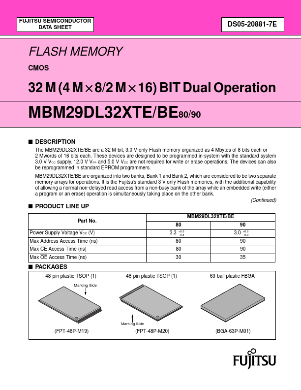
The MBM29DL32XTE/BE are a 32 M-bit, 3.0 V-only Flash memory organized as 4 Mbytes of 8 bits each or 2 Mwords of 16 bits each.
These devices are designed to be programmed in-system with the standard system 3.0 V VCC supply.
12.0 V VPP and 5.0 V VCC are not required for write or erase operations.
| Part number | MBM29DL322TE |
|---|---|
| Manufacturer | Fujitsu Semiconductor Limited |
| File Size | 1.28 MB |
| Description | (MBM29DL32xTE/BE) FLASH MEMORY CMOS 32 M (4 M X 8/2 M X 16) BIT |
| Datasheet |
MBM29DL322TE Datasheet
|
|
|
|
| Part Number | Description | Manufacturer |
|---|---|---|
| MBM29DL322TD-12 | 32M (4M x 8/2M x 16) BIT Dual Operation | Fujitsu |
| MBM29DL322TD-80 | 32M (4M x 8/2M x 16) BIT Dual Operation | Fujitsu |
| MBM29DL322TD-90 | 32M (4M x 8/2M x 16) BIT Dual Operation | Fujitsu |
| MBM29DL322BD-12 | 32M (4M x 8/2M x 16) BIT Dual Operation | Fujitsu |
| MBM29DL322BD-80 | 32M (4M x 8/2M x 16) BIT Dual Operation | Fujitsu |
| Part Number | Description |
|---|---|
| MBM29DL322TD | (MBM29DL32xBD) 32M (4M X 8/2M X 16) BIT Dual Operation |
| MBM29DL322BD | (MBM29DL32xBD) 32M (4M X 8/2M X 16) BIT Dual Operation |
| MBM29DL322BE | (MBM29DL32xTE/BE) FLASH MEMORY CMOS 32 M (4 M X 8/2 M X 16) BIT |
| MBM29DL321BD | (MBM29DL32xBD) 32M (4M X 8/2M X 16) BIT Dual Operation |
| MBM29DL321TD | (MBM29DL32xBD) 32M (4M X 8/2M X 16) BIT Dual Operation |
The following content is an automatically extracted verbatim text from the original manufacturer datasheet and is provided for reference purposes only.