Datasheet4U Logo Datasheet4U.com

MBM29F400TC-55 - 4M (512K x 8/256K x 16) BIT FLASH MEMORY

Download the MBM29F400TC-55 datasheet PDF. This datasheet also covers the MBM29F400BC variant, as both devices belong to the same 4m (512k x 8/256k x 16) bit flash memory family and are provided as variant models within a single manufacturer datasheet.

Features

  • www. DataSheet4U. com.
  • Single 5.0 V read, write, and erase Minimizes system level power requirements.
  • Compatible with JEDEC-standard commands Uses same software commands as E2PROMs.
  • Compatible with JEDEC-standard world-wide pinouts 48-pin TSOP (Package suffix: PFTN.
  • Normal Bend Type, PFTR.
  • Reversed Bend Type) 44-pin SOP (Package suffix: PF).
  • Minimum 100,000 write/erase cycles.
  • High performance 55 ns maximum access time.
  • Sect.

📥 Download Datasheet

Note: The manufacturer provides a single datasheet file (MBM29F400BC_FujitsuMediaDevices.pdf) that lists specifications for multiple related part numbers.

Full PDF Text Transcription (Reference)

The following content is an automatically extracted verbatim text from the original manufacturer datasheet and is provided for reference purposes only.

View original datasheet text
FUJITSU SEMICONDUCTOR DATA SHEET DS05-20851-4E FLASH MEMORY CMOS 4M (512K × 8/256K × 16) BIT MBM29F400TC-55/-70/-90/MBM29F400BC-55/-70/-90 s FEATURES www.DataSheet4U.com • Single 5.0 V read, write, and erase Minimizes system level power requirements • Compatible with JEDEC-standard commands Uses same software commands as E2PROMs 
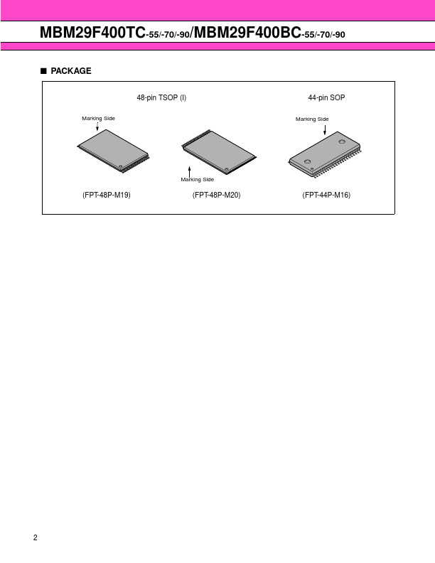
• Compatible with JEDEC-standard world-wide pinouts 48-pin TSOP (Package suffix: PFTN – Normal Bend Type, PFTR – Reversed Bend Type) 44-pin SOP (Package suffix: PF) • Minimum 100,000 write/erase cycles • High performance 55 ns maximum access time • Sector erase architecture One 16K byte, two 8K bytes, one 32K byte, and seven 64K bytes. Any combination of sectors can be concurrently erased. Also supports full chip erase.
Published: |