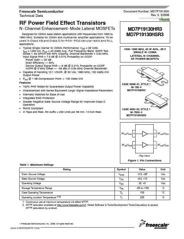
Datasheet4U Logo Datasheet4U.com

MD7P19130HR3 - RF Power Field Effect Transistors

Description

Short Ferrite Bead 47 μF, 50 V Electrolytic Capacitor 100 μF, 50 V Electrolitic Capacitor 1.0 μF Chip Capacitor 0.1 μF Chip Capacitors 11 pF Chip Capacitors 13 pF Chip Capacitor 8.2 pF Chip Capacitor 22 μF, 35 V Tantalum Capacitor 470 μF, 63 V Electrolytic Capacitor 10 μF, 50 V Chip Capacitor 10 Ω,

Features

  • 100% PAR Tested for Guaranteed Output Power Capability.
  • Characterized with Series Equivalent Large - Signal Impedance Parameters.
  • Internally Matched for Ease of Use.
  • Integrated ESD Protection.
  • Greater Negative Gate - Source Voltage Range for Improved Class C Operation.
  • RoHS Compliant.
  • In Tape and Reel. R3 Suffix = 250 Units per 56 mm, 13 inch Reel. MD7P19130HR3 MD7P19130HSR3 1930 - 1990 MHz, 40 W AVG. , 28 V SINGLE W - CDMA.

📥 Download Datasheet

Datasheet preview – MD7P19130HR3

Datasheet Details

Part number MD7P19130HR3
Manufacturer Freescale Semiconductor
File Size 530.11 KB
Description RF Power Field Effect Transistors
Datasheet download datasheet MD7P19130HR3 Datasheet
Additional preview pages of the MD7P19130HR3 datasheet.
Other Datasheets by Freescale Semiconductor

Full PDF Text Transcription

Click to expand full text
Freescale Semiconductor Technical Data Document Number: MD7P19130H Rev. 0, 5/2008 www.DataSheet4U.com RF Power Field Effect Transistors N - Channel Enhancement - Mode Lateral MOSFETs Designed for CDMA base station applications with frequencies from 1930 to 1990 MHz. Suitable for CDMA and multicarrier amplifier applications. To be used in Class AB and Class C for PCN - PCS/cellular radio and WLL applications. • Typical Single - Carrier W - CDMA Performance: VDD = 28 Volts, IDQ = 1250 mA, Pout = 40 Watts Avg., Full Frequency Band, 3GPP Test Model 1, 64 DPCH with 50% Clipping, Channel Bandwidth = 3.84 MHz, Input Signal PAR = 7.5 dB @ 0.01% Probability on CCDF. Power Gain — 20 dB Drain Efficiency — 30% Device Output Signal PAR — 6 dB @ 0.
Published: |