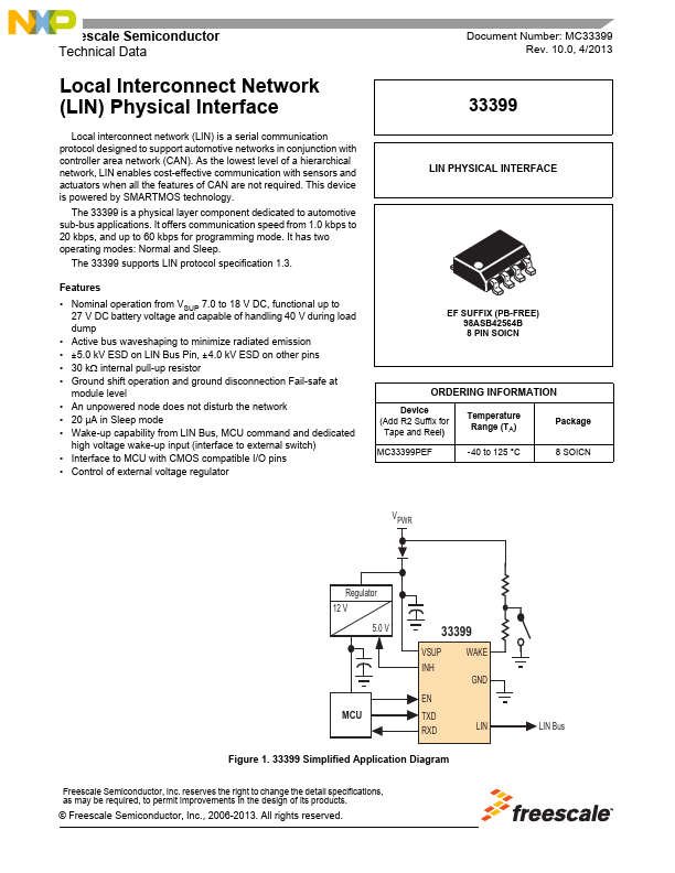
33399 Overview
Key Features
- Nominal operation from VSUP 7.0 to 18 V DC, functional up to 27 V DC battery voltage and capable of handling 40 V during load dump
- Active bus waveshaping to minimize radiated emission
- ±5.0 kV ESD on LIN Bus Pin, ±4.0 kV ESD on other pins
- 30 k internal pull-up resistor
- Ground shift operation and ground disconnection Fail-safe at module level
- An unpowered node does not disturb the network
- 20 µA in Sleep mode
- Wake-up capability from LIN Bus, MCU command and dedicated high voltage wake-up input (interface to external switch)
- Interface to MCU with CMOS compatible I/O pins
- Control of external voltage regulator LIN PHYSICAL INTERFACE EF SUFFIX (PB-FREE) 98ASB42564B 8 PIN SOICN