SL24-M Key Features
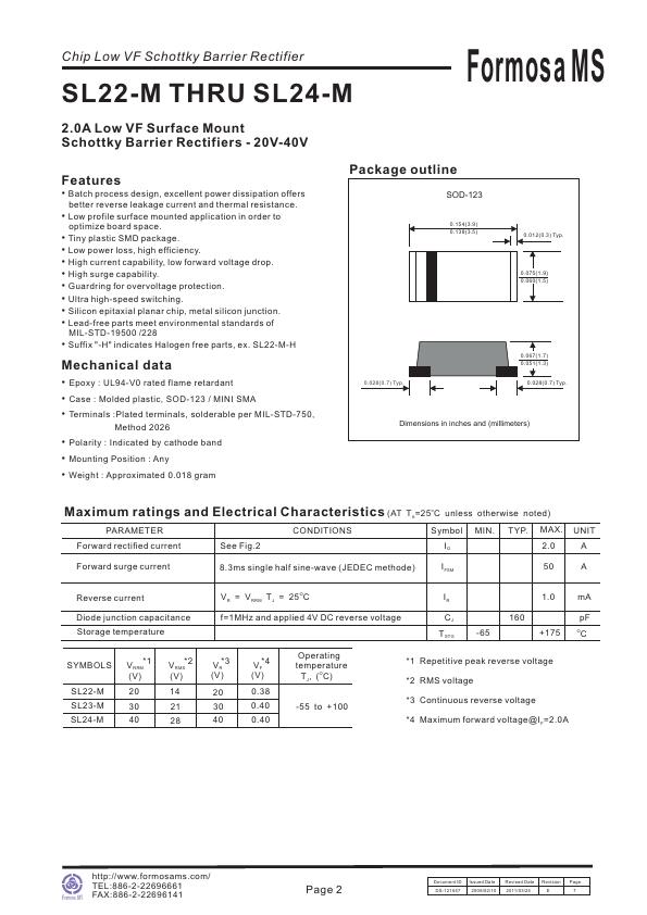
- 2 Mechanical data
- 2 Maximum ratings
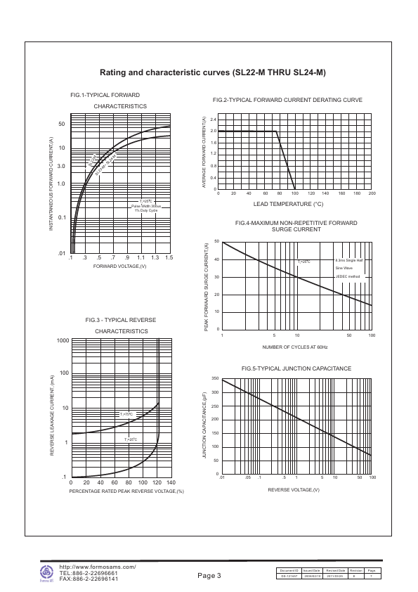
- 2 Rating and characteristic curves
- 3 Pinning information
- 4 Marking
- 4 Suggested solder pad layout
- 4 Packing information
| Manufacturer | Part Number | Description |
|---|---|---|
| SL24-L | 2.0A LOW VF SCHOTTKY BARRIER RECTIFIERS | |
| SL24 | Surface Mount Schottky Barrier Rectifier | |
| SL24 | 2.0A LOW VF SURFACE MOUNT SCHOTTKY BARRIER RECTIFIER | |
| SL24 | Low Capacitance TVS Diode | |
| Crownpo Crownpo |
SL24 | Low VF Chip Schottky Barrier Rectifier |