The following content is an automatically extracted verbatim text
from the original manufacturer datasheet and is provided for reference purposes only.
View original datasheet text
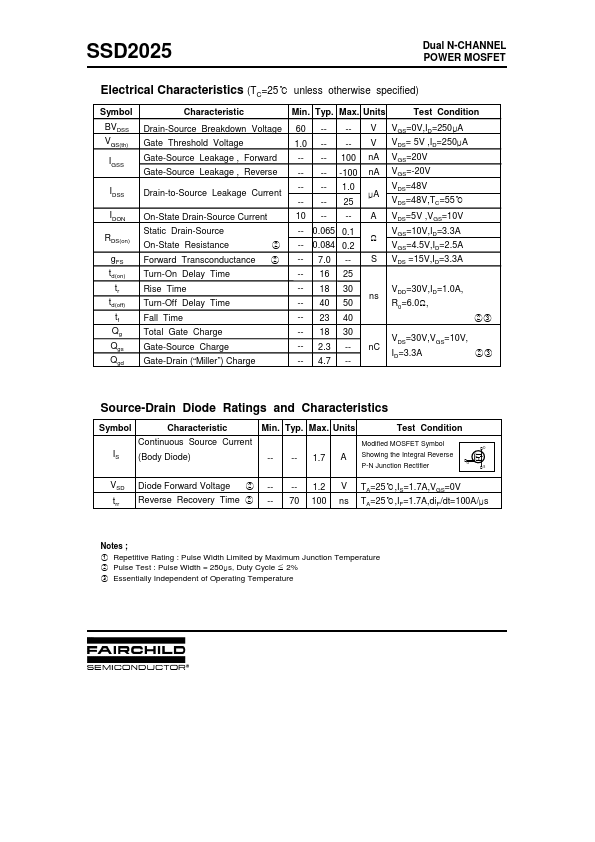
Dual N-CHANNEL POWER MOSFET
FEATURES
! Lower RDS(on) ! Improved Inductive Ruggedness ! Fast Switching Times ! Low Input Capacitance ! Extended Safe Operating Area ! Improved High Temperature Reliability
G1 ,G2 ▼ ▼
SSD2025
8 SOIC
S1 G1 S2 G2
1 2 3 4 8 7 6 5
D1 D1 D2 D2
Top View
D1,D2
D1,D2
Product Summary
Part Number SSD2025 BVDSS 60V RDS(on) 0.10Ω ID 3.3A
S1 ,S2
N -Channel MOSFET
Absolute Maximum Ratings
Symbol VDSS ID IDM VGS PD TJ , TSTG Characteristic Drain-to-Source Voltage Continuous Drain Current TA=25℃ Continuous Drain Current TA=70℃ Drain Current-Pulsed Gate-to-Source Voltage Total Power Dissipation ( TA=25℃ ) ( TA=70℃ ) Operating and Junction Storage Temperature Range ① Value 60 3.3 2.6 10.0 ±20 2.0 1.
 SSD2025 Datasheet