Datasheet4U Logo Datasheet4U.com

IRFI614B - N-Channel MOSFET

Download the IRFI614B datasheet PDF. This datasheet also covers the IRFW614B variant, as both devices belong to the same n-channel mosfet family and are provided as variant models within a single manufacturer datasheet.
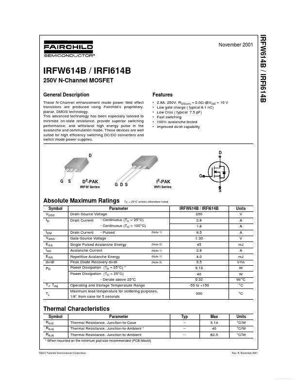
Description

These N-Channel enhancement mode power field effect transistors are produced using Fairchild’s proprietary, planar, DMOS technology.

Features

  • 2.8A, 250V, RDS(on) = 2.0Ω @VGS = 10 V Low gate charge ( typical 8.1 nC) Low Crss ( typical 7.5 pF) Fast switching 100% avalanche tested Improved dv/dt capability D D !.
  • ◀ ▲.
  • G! G S D2-PAK IRFW Series G D S I2-PAK IRFI Series ! S 
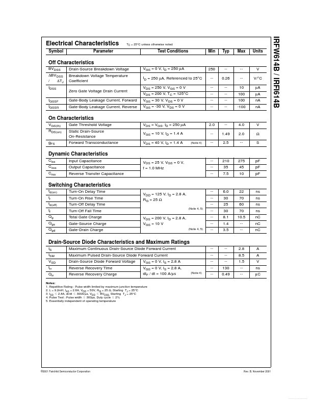
Absolute Maximum Ratings Symbol VDSS ID IDM VGSS EAS IAR EAR dv/dt PD TC = 25°C unless otherwise noted Parameter Drain-Source Voltage - Continuous (TC = 25°C) Drain Current - Continu.

📥 Download Datasheet

Note: The manufacturer provides a single datasheet file (IRFW614B_FairchildSemiconductor.pdf) that lists specifications for multiple related part numbers.

Full PDF Text Transcription (Reference)

The following content is an automatically extracted verbatim text from the original manufacturer datasheet and is provided for reference purposes only.

View original datasheet text
IRFW614B / IRFI614B November 2001 IRFW614B / IRFI614B 250V N-Channel MOSFET General Description These N-Channel enhancement mode power field effect transistors are produced using Fairchild’s proprietary, planar, DMOS technology. This advanced technology has been especially tailored to minimize on-state resistance, provide superior switching performance, and withstand high energy pulse in the avalanche and commutation mode. These devices are well suited for high efficiency switching DC/DC converters and switch mode power supplies. Features • • • • • • 2.8A, 250V, RDS(on) = 2.0Ω @VGS = 10 V Low gate charge ( typical 8.1 nC) Low Crss ( typical 7.