Datasheet Details
| Part number | FM24C04U |
|---|---|
| Manufacturer | Fairchild (onsemi) |
| File Size | 105.71 KB |
| Description | 4K-Bit Standard 2-Wire Bus Interface Serial EEPROM |
| Datasheet |
 FM24C04U Datasheet FM24C04U Datasheet
|
|
|
Download the FM24C04U datasheet PDF. This datasheet also covers the FM2 variant, as both devices belong to the same 4k-bit standard 2-wire bus interface serial eeprom family and are provided as variant models within a single manufacturer datasheet.
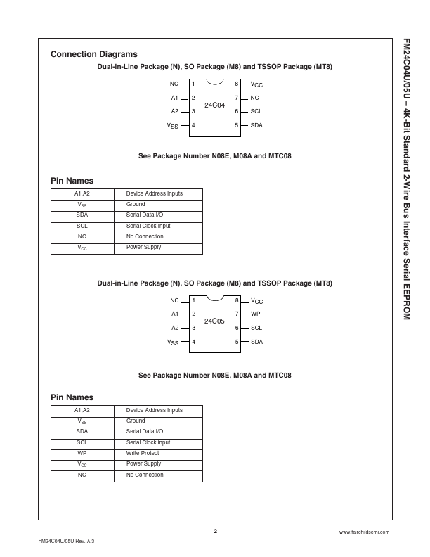
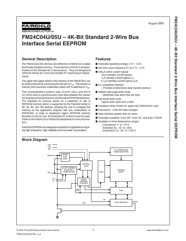
The FM24C04U/05U devices are 4096 bits of CMOS non-volatile electrically erasable memory.
These devices conform to all specifications in the Standard IIC 2-wire protocol.
They are designed to minimize device pin count and simplify PC board layout requirements.
| Part number | FM24C04U |
|---|---|
| Manufacturer | Fairchild (onsemi) |
| File Size | 105.71 KB |
| Description | 4K-Bit Standard 2-Wire Bus Interface Serial EEPROM |
| Datasheet |
FM24C04U Datasheet
|
|
|
|
| Part Number | Description | Manufacturer |
|---|---|---|
| FM24C04 | 2-Wire Serial EEPROM | Fudan |
| FM24C04A | 4Kb FRAM Serial Memory | Ramtron |
| FM24C04B | 4-Kbit (512 x 8) Serial (I2C) F-RAM | Cypress Semiconductor |
| FM24C04B | 4Kb Serial 5V F-RAM Memory | Ramtron |
| FM24C04B | 2-Wire Serial EEPROM | Fudan |
| Part Number | Description |
|---|---|
| FM24C02U | 2K-Bit Standard 2-Wire Bus Interface Serial EEPROM |
| FM24C03U | 2K-Bit Standard 2-Wire Bus Interface Serial EEPROM |
| FM24C05U | 4K-Bit Standard 2-Wire Bus Interface Serial EEPROM |
| FM24C08U | 4K-Bit Standard 2-Wire Bus Interface Serial EEPROM |
| FM24C09U | 8K-Bit Standard 2-Wire Bus Interface Serial EEPROM |
The following content is an automatically extracted verbatim text from the original manufacturer datasheet and is provided for reference purposes only.