FIN1026
Overview
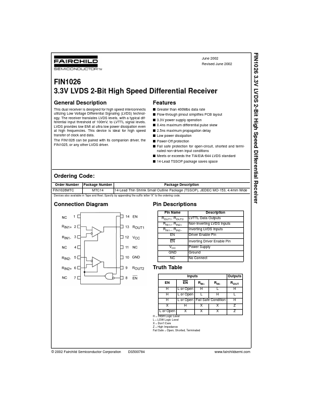
This dual receiver is designed for high speed interconnects utilizing Low Voltage Differential Signaling (LVDS) technology. The receiver translates LVDS levels, with a typical differential input threshold of 100mV, to LVTTL signal levels.