Datasheet Summary
April 2008
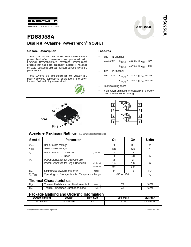
FDS8958A tm
Dual N & P-Channel PowerTrench® MOSFET
General Description
These dual N- and P-Channel enhancement mode power field effect transistors are produced using Fairchild Semiconductor’s advanced PowerTrench process that has been especially tailored to minimize on-state ressitance and yet maintain superior switching performance.
These devices are well suited for low voltage and battery powered applications where low in-line power loss and fast switching are required.
Features
- Q1: N-Channel 7.0A, 30V RDS(on) = 0.028Ω @ VGS = 10V RDS(on) = 0.040Ω @ VGS = 4.5V
- Q2: P-Channel -5A, -30V RDS(on) = 0.052Ω @ VGS = -10V RDS(on) = 0.080Ω @ VGS = -4.5V
- Fast...