Datasheet4U Logo Datasheet4U.com

FDS6898A - Dual N-Channel Logic Level PWM Optimized PowerTrench MOSFET

Description

These N-Channel Logic Level MOSFETs are produced using Fairchild Semiconductor’s advanced PowerTrench process that has been especially tailored to minimize the on-state resistance and yet maintain superior switching performance.

Features

  • 9.4 A, 20 V RDS(ON) = 14 mΩ @ VGS = 4.5 V RDS(ON) = 18 mΩ @ VGS = 2.5 V.
  • Low gate charge (16 nC typical).
  • High performance trench technology for extremely low RDS(ON).
  • High power and current handling capability D2 D D2 D DD1 D1 D 5 6 7 Q1 4 3 2 Q2 SO-8 Pin 1 SO-8 G2 S2 S G1 S1 G S 8 1 S Absolute Maximum Ratings Symbol VDSS VGSS ID PD Drain-Source Voltage Gate-Source Voltage Drain Current.
  • Continuous.
  • Pulsed TA=25 C unless other.

📥 Download Datasheet

Full PDF Text Transcription (Reference)

The following content is an automatically extracted verbatim text from the original manufacturer datasheet and is provided for reference purposes only.

View original datasheet text
FDS6898A OCTOBER 2001 FDS6898A 
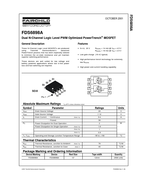
Dual N-Channel Logic Level PWM Optimized PowerTrench® MOSFET General Description These N-Channel Logic Level MOSFETs are produced using Fairchild Semiconductor’s advanced PowerTrench process that has been especially tailored to minimize the on-state resistance and yet maintain superior switching performance. These devices are well suited for low voltage and battery powered applications where low in-line power loss and fast switching are required. Features • 9.4 A, 20 V RDS(ON) = 14 mΩ @ VGS = 4.5 V RDS(ON) = 18 mΩ @ VGS = 2.
Published: |