FDS4435
Description
This P-Channel MOSFET is a rugged gate version of Fairchild Semiconductor’s advanced Power Trench process. It has been optimized for power management applications requiring a wide range of gave drive voltage ratings (4.5V
- 25V).
Applications
- Power management
- Load switch
- Battery protection
Features
- - 8.8 A,
- 30 V
RDS(ON) = 20 mΩ @ VGS =
- 10 V RDS(ON) = 35 mΩ @ VGS =
- 4.5 V
- Low gate charge (17n C typical)
- Fast switching speed
- High performance trench technology for extremely low RDS(ON)
- High power and current handling capability
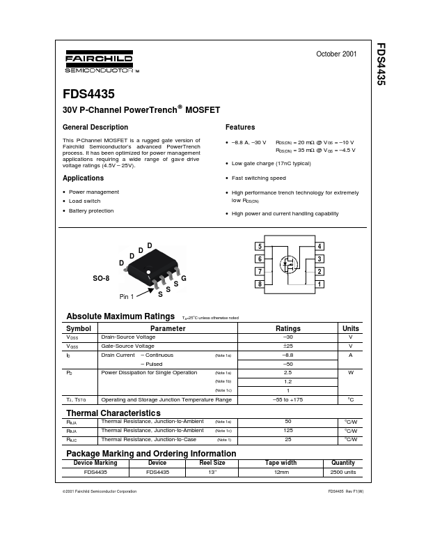
DD DD DD DD
SO-8
Pin 1SO-8 SS SS SS GG
Absolute Maximum Ratings TA=25o C unless otherwise noted
Symbol
VDSS V GSS ID
Parameter
Drain-Source Voltage Gate-Source Voltage Drain Current
- Continuous
- Pulsed Power Dissipation for Single Operation
(Note 1a)
(Note 1a) (Note 1b)
TJ, TSTG
(Note 1c)
Operating and Storage Junction Temperature Range
Thermal Characteristics
RθJA Thermal Resistance, Junction-to-Ambient RθJA Thermal...