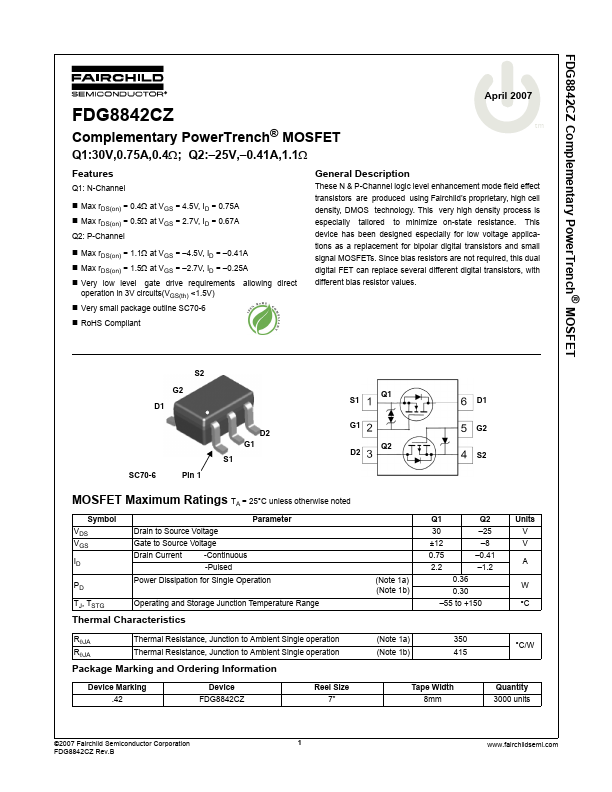
Datasheet4U Logo Datasheet4U.com

FDG8842CZ - MOSFET

General Description

These N & P-Channel logic level enhancement mode field effect transistors are produced using Fairchild’s proprietary, high cell density, DMOS technology.

This very high density process is especially tailored to minimize on-state resistance.

Key Features

  • Q1: N-Channel.
  • Max rDS(on) = 0.4Ω at VGS = 4.5V, ID = 0.75A.
  • Max rDS(on) = 0.5Ω at VGS = 2.7V, ID = 0.67A Q2: P-Channel.
  • Max rDS(on) = 1.1Ω at VGS =.
  • 4.5V, ID =.
  • 0.41A.
  • Max rDS(on) = 1.5Ω at VGS =.
  • 2.7V, ID =.
  • 0.25A.
  • Very low level gate drive requirements allowing direct operation in 3V circuits(VGS(th).

📥 Download Datasheet

Full PDF Text Transcription for FDG8842CZ (Reference)

Note: Below is a high-fidelity text extraction (approx. 800 characters) for FDG8842CZ. For precise diagrams, and layout, please refer to the original PDF.

FDG8842CZ Complementary PowerTrench® MOSFET FDG8842CZ Complementary PowerTrench® MOSFET April 2007 tm Q1:30V,0.75A,0.4Ω; Q2:–25V,–0.41A,1.1Ω Features Q1: N-Channel „ Max ...

View more extracted text
m Q1:30V,0.75A,0.4Ω; Q2:–25V,–0.41A,1.1Ω Features Q1: N-Channel „ Max rDS(on) = 0.4Ω at VGS = 4.5V, ID = 0.75A „ Max rDS(on) = 0.5Ω at VGS = 2.7V, ID = 0.67A Q2: P-Channel „ Max rDS(on) = 1.1Ω at VGS = –4.5V, ID = –0.41A „ Max rDS(on) = 1.5Ω at VGS = –2.7V, ID = –0.25A „ Very low level gate drive requirements allowing direct operation in 3V circuits(VGS(th) <1.5V) „ Very small package outline SC70-6 General Description These N & P-Channel logic level enhancement mode field effect transistors are produced using Fairchild’s proprietary, high cell density, DMOS technology. This very high density process is especially tailored