FDG6321C Overview
Key Specifications
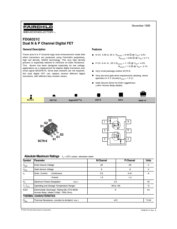
Package: SC
Mount Type: Surface Mount
Pins: 6
Height: 1.1 mm
Description
These dual N & P-Channel logic level enhancement mode field effect transistors are produced using Fairchild's proprietary, high cell density, DMOS technology. This very high density process is especially tailored to minimize on-state resistance.
Key Features
- N-Ch 0.50 A, 25 V, RDS(ON) = 0.45 Ω @ VGS= 4.5V
- RDS(ON) = 0.60 Ω @ VGS= 2.7 V
- P-Ch -0.41 A, -25 V,RDS(ON) = 1.1 Ω @ VGS= -4.5V
- RDS(ON) = 1.5 Ω @ VGS= -2.7V
- Very small package outline SC70-6