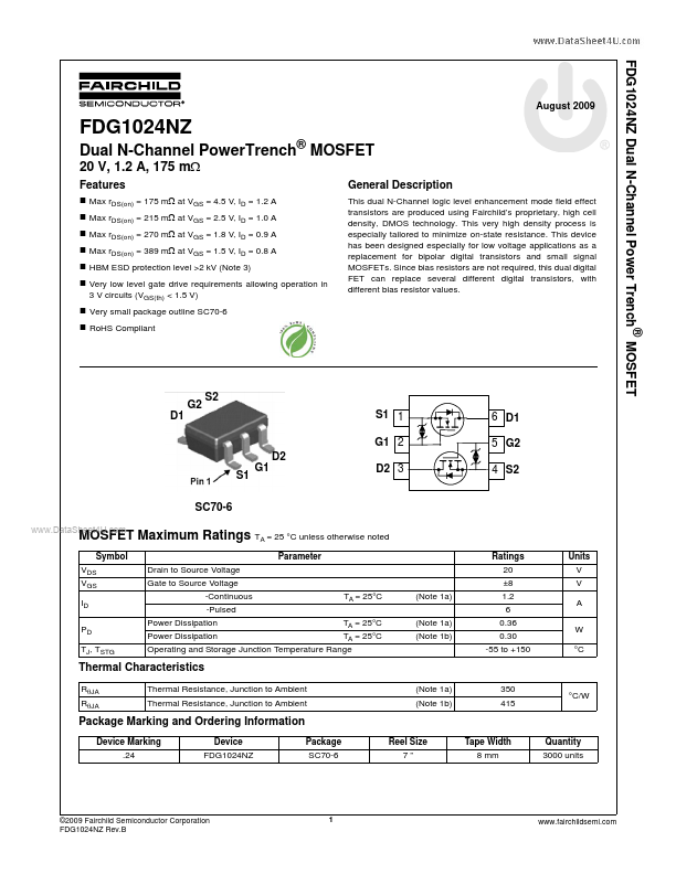
Datasheet4U Logo Datasheet4U.com

FDG1024NZ - N-Channel MOSFET

General Description

This dual N-Channel logic level enhancement mode field effect transistors are produced using Fairchild’s proprietary, high cell density, DMOS technology.

This very high density process is especially tailored to minimize on-state resistance.

Key Features

  • Max rDS(on) = 175 mΩ at VGS = 4.5 V, ID = 1.2 A.
  • Max rDS(on) = 215 mΩ at VGS = 2.5 V, ID = 1.0 A.
  • Max rDS(on) = 270 mΩ at VGS = 1.8 V, ID = 0.9 A.
  • Max rDS(on) = 389 mΩ at VGS = 1.5 V, ID = 0.8 A.
  • HBM ESD protection level >2 kV (Note 3).
  • Very low level gate drive requirements allowing operation in 3 V circuits (VGS(th) < 1.5 V).
  • Very small package outline SC70-6.
  • RoHS Compliant General.

📥 Download Datasheet

Full PDF Text Transcription (Reference)

The following content is an automatically extracted verbatim text from the original manufacturer datasheet and is provided for reference purposes only.

View original datasheet text
FDG1024NZ Dual N-Channel Power Trench® MOSFET August 2009 FDG1024NZ Dual N-Channel PowerTrench® MOSFET 20 V, 1.2 A, 175 mΩ Features „ Max rDS(on) = 175 mΩ at VGS = 4.5 V, ID = 1.2 A „ Max rDS(on) = 215 mΩ at VGS = 2.5 V, ID = 1.0 A „ Max rDS(on) = 270 mΩ at VGS = 1.8 V, ID = 0.9 A „ Max rDS(on) = 389 mΩ at VGS = 1.5 V, ID = 0.8 A „ HBM ESD protection level >2 kV (Note 3) „ Very low level gate drive requirements allowing operation in 3 V circuits (VGS(th) < 1.5 V) „ Very small package outline SC70-6 „ RoHS Compliant General Description This dual N-Channel logic level enhancement mode field effect transistors are produced using Fairchild’s proprietary, high cell density, DMOS technology. This very high density process is especially tailored to minimize on-state resistance.