FDD6632
FDD6632 is N-Channel MOSFET manufactured by Fairchild Semiconductor.
Description
This device employs a new advanced trench MOSFET technology and features low gate charge while maintaining low on-resistance. Optimized for switching applications, this device improves the overall efficiency of DC/DC converters and allows operation to higher switching frequencies. Formerly developmental type 83317
Features
- Fast switching
- r DS(ON) = 0.058Ω (Typ), VGS = 10V, ID = 9A
- r DS(ON) = 0.090Ω (Typ), VGS = 4.5V, ID = 6A
- Qg(TOT) (Typ) = 2.6n C, VGS = 5V
- Qgd (Typ) = 0.8n C
- CISS (Typ) = 255p F
Applications
- DC/DC converters
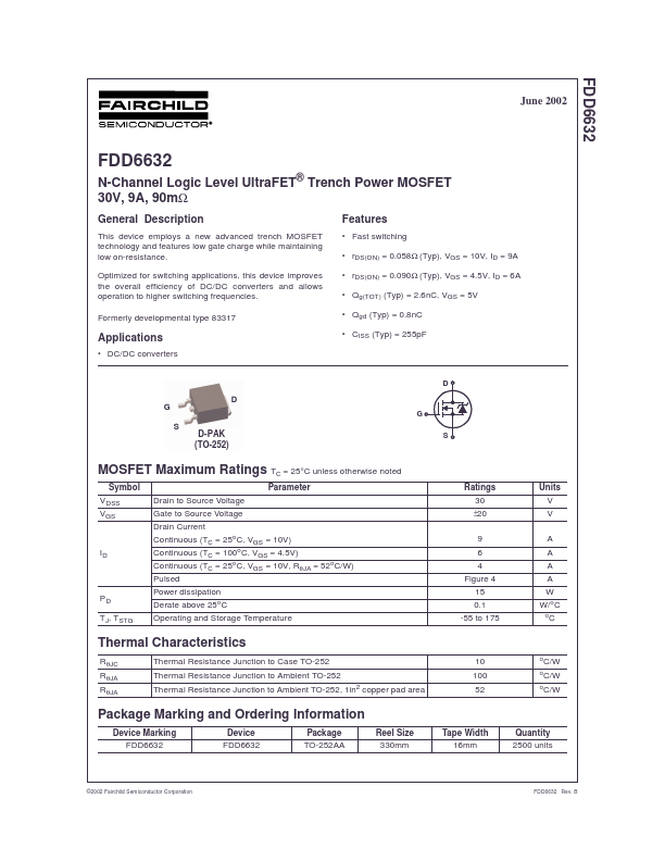
D-PAK TO-252 (TO-252)
MOSFET Maximum Ratings TC = 25°C unless otherwise noted
Symbol VDSS VGS Parameter Drain to Source Voltage Gate to Source Voltage Drain Current Continuous (TC = 25o C, VGS = 10V) ID Continuous (TC = 100o C, VGS = 4.5V) Continuous (TC = 25o C, VGS = 10V, Rθ JA = 52o C/W) Pulsed PD TJ, TSTG Power dissipation Derate above 25o C Operating and Storage Temperature 9 6 4 Figure 4 15 0.1 -55 to 175 A A A A W W/o C o
Ratings 30 ±20
Units V V
Thermal Characteristics
Rθ JC Rθ JA Rθ JA Thermal Resistance Junction to Case TO-252 Thermal Resistance Junction to Ambient TO-252 Thermal Resistance Junction to Ambient TO-252, 1in2 copper pad area 10 100 52 o o
C/W C/W o C/W
Package Marking and Ordering Information
Device Marking FDD6632 Device FDD6632 Package TO-252AA Reel Size 330mm Tape Width 16mm Quantity 2500 units
©2002 Fairchild Semiconductor Corporation
FDD6632 Rev. B
Electrical Characteristics TC = 25°C unless otherwise noted
Symbol Parameter Test Conditions Min Typ Max Units
Off Characteristics
BVDSS IDSS IGSS Drain to Source Breakdown Voltage Zero Gate Voltage Drain Current Gate to Source Leakage Current ID = 250µA, VGS = 0V VDS = 25V VGS = 0V VGS = ±20V TC = 150o C 30 1 250 ±100 V µA n A
On Characteristics
VGS(TH) r DS(ON) Gate to Source Threshold Voltage Drain to Source On Resistance VGS = VDS, ID = 250µA ID = 9A, VGS = 10V ID = 6A, VGS = 4.5V 1 0.058 0.090 3 0.090 0.110 V...