FDD3N50NZ Overview
Key Specifications
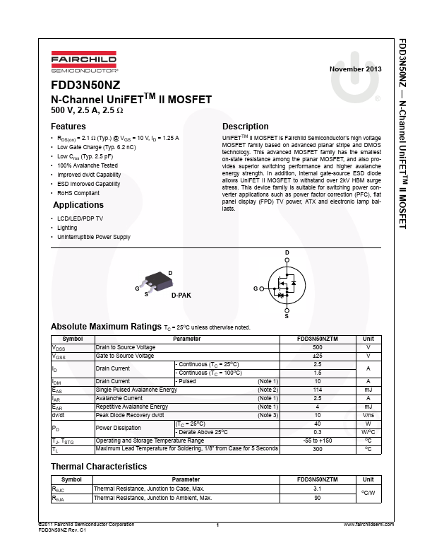
Package: DPAK
Mount Type: Surface Mount
Pins: 3
Height: 2.39 mm
Description
UniFETTM II MOSFET is Fairchild Semiconductor’s high voltage MOSFET family based on advanced planar stripe and DMOS technology. This advanced MOSFET family has the smallest on-state resistance among the planar MOSFET, and also provides superior switching performance and higher avalanche energy strength.
Key Features
- RDS(on) = 2.1 Ω (Typ.) @ VGS = 10 V, ID = 1.25 A
- Low Gate Charge (Typ. 6.2 nC)
- Low Crss (Typ. 2.5 pF)
- 100% Avalanche Tested
- Improved dv/dt Capability