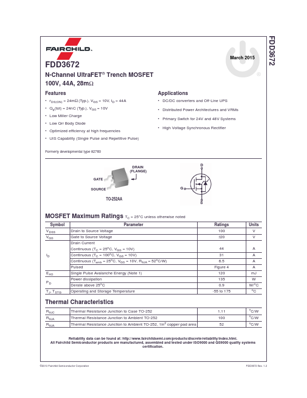
Download FDD3672 Datasheet PDF
Fairchild Semiconductor
FDD3672
Features - r DS(ON) = 24mΩ (Typ.), VGS = 10V, ID = 44A - Qg(tot) = 24n C (Typ.), VGS = 10V - Low Miller Charge - Low Qrr Body Diode - Optimized efficiency at high frequencies - UIS Capability (Single Pulse and Repetitive Pulse) Applications - DC/DC converters and Off-Line UPS - Distributed Power Architectures and VRMs - Primary Switch for 24V and 48V Systems - High Voltage Synchronous Rectifier Formerly developmental type 82760 GATE DRAIN (FLANGE) SOURCE TO-252AA MOSFET Maximum Ratings TC = 25°C unless otherwise noted Symbol VDSS VGS EAS PD TJ, TSTG Parameter Drain to Source Voltage Gate to Source Voltage Drain Current Continuous (TC = 25o C, VGS = 10V) Continuous (TC = 100o C, VGS = 10V) Continuous (Tamb = 25o C, VGS = 10V, RθJA = 52o C/W) Pulsed Single Pulse Avalanche Energy (Note 1) Power dissipation Derate above 25o C Operating and Storage Temperature Thermal Characteristics RθJC RθJA RθJA Thermal Resistance Junction to Case TO-252 Thermal Resistance Junction to...