FDC6321C
FDC6321C is Dual N & P Channel / Digital FET manufactured by Fairchild Semiconductor.
Description
These dual N & P Channel logic level enhancement mode field effect transistors are produced using Fairchild's proprietary, high cell density, DMOS technology. This very high density process is especially tailored to minimize on-state resistance. This device has been designed especially for low voltage applications as a replacement for digital transistors in load switching applications. Since bias resistors are not required this dual digital FET can replace several digital transistors with different bias resistors.
Features
N-Ch 25 V, 0.68 A, RDS(ON) = 0.45 Ω @ VGS= 4.5 V P-Ch -25 V, -0.46 A, RDS(ON) = 1.1 Ω @ VGS= -4.5 V. Very low level gate drive requirements allowing direct operation in 3 V circuits. VGS(th) < 1.0V. Gate-Source Zener for ESD ruggedness. >6k V Human Body Model Replace multiple dual NPN & PNP digital transistors.
SOT-23
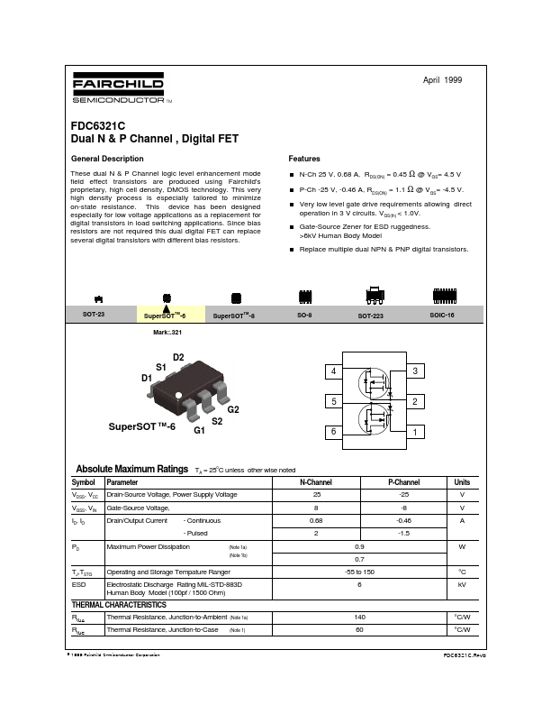
Super SOTTM-6 Mark:.321
Super SOTTM-8
SO-8
SOT-223
SOIC-16
D2 S1 D1
4 3
G2
Super SOT TM -6
S2 G1
6 1
Absolute Maximum Ratings
Symbol Parameter
TA = 25o C unless other wise noted
N-Channel P-Channel Units
VDSS, VCC VGSS, VIN ID, IO PD TJ,TSTG ESD
Drain-Source Voltage, Power Supply Voltage Gate-Source Voltage, Drain/Output Current
- Continuous
- Pulsed Maximum Power Dissipation
(Note 1a) (Note 1b)
25 8 0.68 2 0.9 0.7 -55 to 150 6
-25 -8 -0.46 -1.5
Operating and Storage Tempature Ranger Electrostatic Discharge Rating MIL-STD-883D Human Body Model (100pf / 1500 Ohm) Thermal Resistance, Junction-to-Ambient Thermal Resistance, Junction-to-Case
°C k V
THERMAL CHARACTERISTICS
RθJA RθJC
(Note 1a) (Note 1)
140 60
°C/W °C/W
© 1999 Fairchild Semiconductor Corporation
FDC6321C.Rev B
Electrical Characteristics (TA = 25 OC unless otherwise noted...