Download CD4069UBC Datasheet PDF
Fairchild Semiconductor
CD4069UBC
CD4069UBC is Inverter Circuits manufactured by Fairchild Semiconductor.
Description 
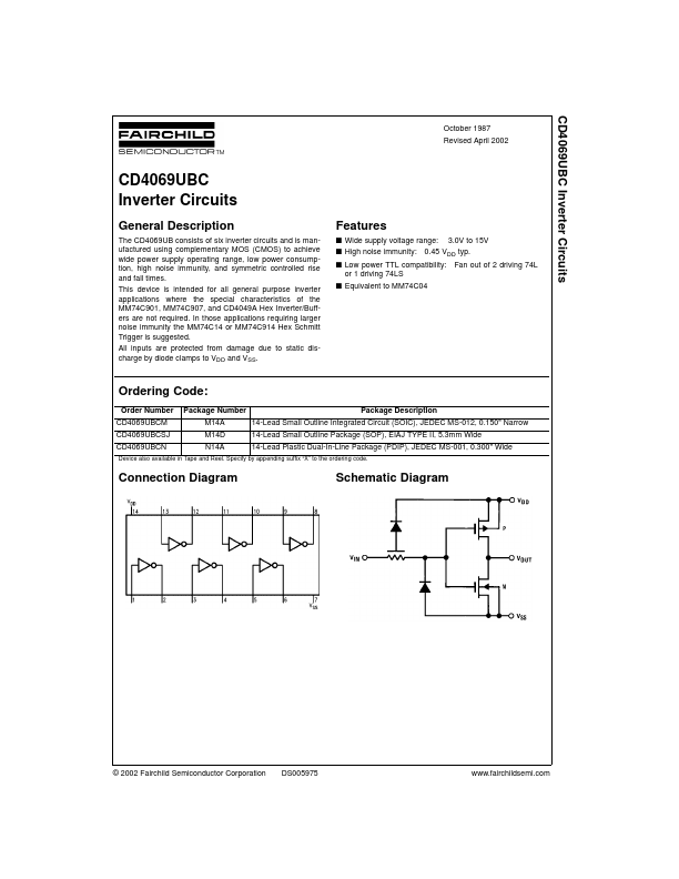
The CD4069UB consists of six inverter circuits and is manufactured using plementary MOS (CMOS) to achieve wide power supply operating range, low power consumption, high noise immunity, and symmetric controlled rise and fall times. This device is intended for all general purpose inverter applications where the special characteristics of the MM74C901, MM74C907, and CD4049A Hex Inverter/Buffers are not required. In those applications requiring larger noise immunity the MM74C14 or MM74C914 Hex Schmitt Trigger is suggested. All inputs are protected from damage due to static discharge by diode clamps to VDD and VSS. Features s Wide supply voltage range: 3.0V to 15V s High noise immunity: 0.45 VDD typ. s Low power TTL patibility: Fan out of 2 driving 74L or 1 driving 74LS s Equivalent to MM74C04 Ordering Code: Order Number Package Number Package Description CD4069UBCM M14A 14-Lead Small Outline Integrated Circuit (SOIC), JEDEC MS-012, 0.150" Narrow CD4069UBCSJ M14D 14-Lead Small Outline Package (SOP), EIAJ TYPE II, 5.3mm Wide CD4069UBCN N14A 14-Lead Plastic Dual-In-Line Package (PDIP), JEDEC MS-001, 0.300" Wide Device also available in Tape and Reel. Specify by appending suffix “X” to the ordering code. Connection Diagram Schematic Diagram © 2002 Fairchild Semiconductor Corporation DS005975 .fairchildsemi. Absolute Maximum Ratings(Note 1) (Note 2) Remended Operating Conditions (Note 2) DC Supply Voltage (VDD) Input Voltage (VIN) Storage Temperature Range (TS) Power Dissipation (PD) Dual-In-Line Small Outline Lead Temperature (TL) (Soldering, 10 seconds) - 0.5V to +18 VDC - 0.5V to VDD +0.5 VDC - 65°C to +150°C 700 m W 500 m W 260°C DC Supply Voltage (VDD) 3V to 15VDC Input Voltage (VIN) 0V to VDD VDC Operating Temperature Range (TA) - 55°C to...