Datasheet4U Logo Datasheet4U.com

CD4027BCM - Dual J-K Master/Slave Flip-Flop

Download the CD4027BCM datasheet PDF (CD4027BC included). The manufacturer datasheet provides complete specifications, pinout details, electrical characteristics, and typical applications for dual j-k master/slave flip-flop.

Description

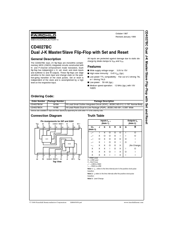
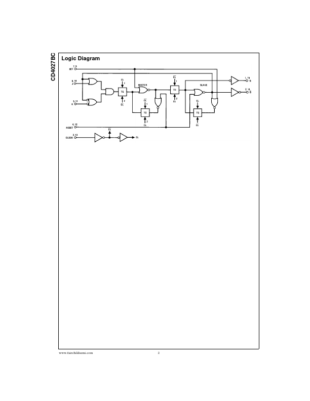
The CD4027BC dual J-K flip-flops are monolithic complementary MOS (CMOS) integrated circuits constructed with N- and P-channel enhancement mode transistors.

Each flip-flop has independent J, K, set, reset, and clock inputs and buffered Q and Q outputs.

Features

  • s Wide supply voltage range: s High noise immunity: 3.0V to 15V 0.45 VDD (typ. ) s Low power TTL compatibility: Fan out of 2 driving 74L or 1 driving 74LS s Low power: 50 nW (typ. ) s Medium speed operation: 12 MHz (typ. ) with 10V supply Ordering Code: Order Number CD4027BCM CD4027BCN Package Number M16A N16E Package.

📥 Download Datasheet

Note: The manufacturer provides a single datasheet file (CD4027BC-FairchildSemiconductor.pdf) that lists specifications for multiple related part numbers.
Other Datasheets by Fairchild Semiconductor

Full PDF Text Transcription

Click to expand full text
CD4027BC Dual J-K Master/Slave Flip-Flop with Set and Reset October 1987 Revised January 1999 CD4027BC Dual J-K Master/Slave Flip-Flop with Set and Reset General Description The CD4027BC dual J-K flip-flops are monolithic complementary MOS (CMOS) integrated circuits constructed with N- and P-channel enhancement mode transistors. Each flip-flop has independent J, K, set, reset, and clock inputs and buffered Q and Q outputs. These flip-flops are edge sensitive to the clock input and change state on the positive-going transition of the clock pulses. Set or reset is independent of the clock and is accomplished by a high level on the respective input. All inputs are protected against damage due to static discharge by diode clamps to VDD and VSS.
Published: |