CD4027BC
CD4027BC is Dual J-K Master/Slave Flip-Flop manufactured by Fairchild Semiconductor.
CD4027BC Dual J-K Master/Slave Flip-Flop with Set and Reset
October 1987 Revised January 1999
CD4027BC Dual J-K Master/Slave Flip-Flop with Set and Reset
General Description
The CD4027BC dual J-K flip-flops are monolithic plementary MOS (CMOS) integrated circuits constructed with N- and P-channel enhancement mode transistors. Each flip-flop has independent J, K, set, reset, and clock inputs and buffered Q and Q outputs. These flip-flops are edge sensitive to the clock input and change state on the positive-going transition of the clock pulses. Set or reset is independent of the clock and is acplished by a high level on the respective input. All inputs are protected against damage due to static discharge by diode clamps to VDD and VSS.
Features s Wide supply voltage range: s High noise immunity: 3.0V to 15V 0.45 VDD (typ.) s Low power TTL patibility: Fan out of 2 driving 74L or 1 driving 74LS s Low power: 50 n W (typ.) s Medium speed operation: 12 MHz (typ.) with 10V supply
Ordering Code:
Order Number CD4027BCM CD4027BCN Package Number M16A N16E Package Description 16-Lead Small Outline Integrated Circuit (SOIC), JEDEC MS-012, 0.150” Narrow Body 16-Lead Plastic Dual-In-Line Package (PDIP), JEDEC MS-001, 0.300” Wide
Devices also available in Tape and Reel. Specify by appending the suffix letter “X” to the ordering code.
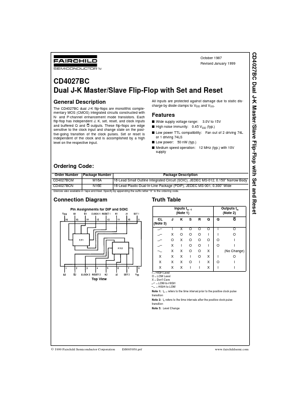
Connection Diagram
Pin Assignments for DIP and SOIC
Truth Table
Inputs tn- 1 (Note 1) CL (Note 3) J I X O X X X X X K X O X I X X X X S O O O O O I O I R O O O O O O I I Q O I O I X X X X I O I Q I I O O Outputs tn (Note 2) Q O O I I (No Change) O I I
Top View
I = HIGH Level O = LOW Level X = Don't Care = LOW-to-HIGH = HIGH-to-LOW
Note 1: tn- 1 refers to the time interval prior to the positive clock pulse transition Note 2: tn refers to the time intervals after the positive clock pulse transition Note 3: Level Change
© 1999 Fairchild Semiconductor Corporation
DS005958.prf
.fairchildsemi.
Logic...